Outline
This procedure outlines the inspection method and pass/fail criteria to be used during the final inspection of BGA Component Deballing and Reballing to ensure compliance with Work Order requirements.
Minimum Skill Level - Expert
Recommended for technicians with advanced soldering and component rework skills and extensive experience in most repair/rework procedures.Conformance Level - High
This procedure most closely duplicates the physical characteristics of the original, and most probably complies with all the functional, environmental and serviceability factors.Tools and Materials
General purpose cleaner for removing contamination. |
|
Cleaning Brushes
Disposable brushes for solvent cleaning and application of coatings. |
Batch or inline cleaning system for removing fluxes and contamination. |
Disposable, puncture-resistant gloves designed for handling mild chemicals. |
Precision microscope with stand and lighting for work and inspection. |
|
Precision Tool Set
Nine precision-crafted tools for detailed circuit board work. |
Nonabrasive, low-linting wipes for cleanup. |
Procedure
Moisture Sensitive Device Control
Before processing, review the requirements for moisture sensitivity.
BGA Inspection Objective
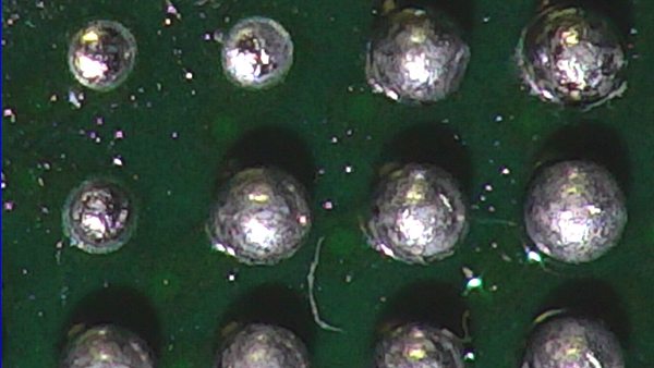
Visual inspection confirms sphere condition, ball alignment, size, and location to ensure the reballing process complies with IPC and JEDEC specifications.
Deballing Inspection Procedure
Components shall be examined for:
- Pad Defects (scratches, etc.)
- Solder Mask Damage
- Residue of the previous alloy
- Flux Residue
- FOD (Foreign Objects and Debris)
Reballing Inspection Procedure
Components shall be examined for:
- Cracks
- Missing Spheres
- Sphere Shape
- Chipouts
- Grazed/Nicked Spheres
- Sphere Placement
- Flux
- Oxidation
- FOD (Foreign Objects and Debris)
- Dimensions per Mechanical Data Sheets
Disposition of Rejected Components
The Material Review Process shall address failed components due to internal or external standards.
Images
BGA Component Reball Inspection
Crushed solder spheres. This is a reject condition.
Excessive flux and oxidation. This is a reject condition.
Substrate damage. This is a reject condition.
Missing solder spheres. This is a reject condition.