Oops! Somebody goofed. Happens all the time.
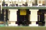
Simple mistakes are magnified on complex, expensive assemblies. A routing miscommunication resulted in a significant problem for a customer. Figure 1 shows how the assembly was actually manufactured. The circuit traces for connectors on the left side were supposed to route to the connectors on the right side. Unfortunately, the opposite was true.
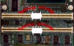
If the circuit board connectors were not rewired and the mating daughter board was plugged in as pictured above, sparks would fly! Due to time considerations, re-manufacturing was not a viable option. Figure 2 shows how the mating connectors should have worked.
There were a few options considered. One option was to manufacture a custom adapter card with the rewired circuit traces. The conductors could have been mounted to the adapter card, and the card could have been soldered to the main circuit board, similar to a leadless chip carrier.
The adapter card option would have involved significant engineering work, and the time constraint would not permit it. The only option meeting the time constraint was good old-fashioned jumper wire rework. In this case, the rework involved four 64-pin connectors requiring 256 wires. That's a lot of wires in a very tight space.
How can you get all these wires in the proper spot without shorting them or connecting them to the wrong pads or connector pins? Well, let's break it down and see how it was done.
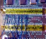
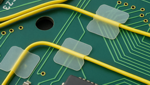
We used the smallest diameter wire to accommodate the tight spacing. A few wires needed a larger gauge for power needs, but the bulk of the wires used were 34 gauge. Figure 3 provides a good view of the mass of wires being put in place.
First, wires were soldered to all the pads on the circuit board surface. Then, thin sections of laminate material the size of the connector were cut, and the connectors were bonded to these laminate sections. These connector and laminate assemblies were then bonded directly over the recently solder jumper wires. It was important to ensure the connectors perfectly aligned with the mating daughter card when the wiring was complete.
Next, the technician began the process of wiring the pads to the proper connector. Each side of each connector's wiring was inspected as it was completed.
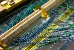
Figure 4 shows the connectors wired to the board.
Piece of cake, can of corn, no problem! (Don't tell that to the technician who slaved over this project for two days.)
Several members of the Circuit Technology Center team contributed to this feature story. Images may be altered or recreated to protect proprietary information.