Outline
This procedure covers the general guidelines for modifications that involve adding components.
Minimum Skill Level - Advanced
Recommended for technicians with soldering and component rework skills and exposure to most repair/rework procedures, but lacking extensive experience.| Procedure References | |
| 1-0 | 1.0 Foreword |
| 2-1 | 2.1 Handling Electronic Assemblies |
| 2-2 | 2.2 Cleaning Procedures |
| 2-5 | 2.5 Baking and Preheating |
| 2-7 | 2.7 Epoxy Mixing and Handling |
| 6-1 | 6.1 Jumper Wires |
Tools and Materials

General purpose cleaner for removing contamination. |

Sturdy rack for PCBs used for rework and positioning. |

Precision microscope with stand and lighting for work and inspection. |

Nine precision-crafted tools for detailed circuit board work. |

Properly maintained soldering iron and properly sized soldering iron tips. |

Nonabrasive, low-linting wipes for cleanup. |
Procedure
General Rules
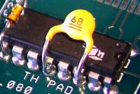
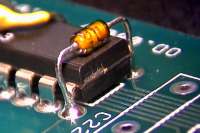
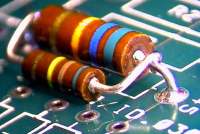
- Added components may need to be secured with adhesive or by other means if the component leads or component body would be subjected to mechanical stress.
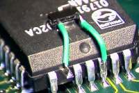
- Leads of added components should not be inserted into plated holes occupied by another component lead.
- Added components placed on the circuit board surface should be placed on the component side of the assembly or circuit board unless otherwise specified.
- Added components shall not be raised above the board surface beyond allowable dimensions.
- Added components shall not cover over pads or vias used as test points.
- Added components shall not cover other component footprints unless the layout of the assembly prohibits mounting in other areas.
- Added component leads may require insulation to avoid contact with the component body or other conductors.
- Removal of existing solder from a connection point may be necessary to avoid bridging, or excess solder, in the final connection.
- Consider design limitations and product use environments when stacking components.
- Do not exceed minimum component lead bend radius.
- When possible, component identification marking shall be legible.
Procedure
- When required, form the component leads and clean the area.
- When required, secure the component in place by bending leads or other mechanical means.
- Apply flux to the joint.
- Place the soldering iron tip at the connection between both leads. Apply a small amount of solder at the connection of the soldering iron tip and lead to form a solder bridge.
- Immediately feed the solder into the joint from the side opposite of the soldering iron tip until the proper fillet is achieved. Remove the solder and iron simultaneously.
- When required, clean the flux residue.
- Inspect
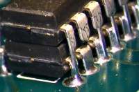
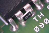
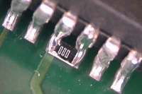
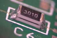
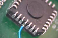
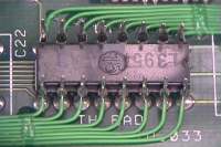
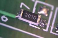
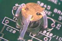
Component Modifications and Additions Figures
 |
 |
 |
 |
 |
 |
 |
 |
 |
 |
 |
 |
Images

Component Modifications and Additions
See the procedure below for detailed instructions.