Some of the odd twists and turns occasionally needed to modify assembled circuit boards can be surprising. Modifications that might seem almost ridiculous or jury-rigged at first glance are often quite acceptable and reliable.
Stacking components, mounting them upside down, or placing them end to end are just a few examples of the wide range of unique modifications that involve components on assembled circuit boards.
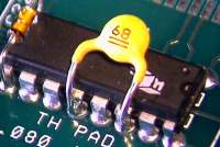
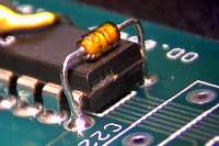
Figures 1 and 2 depict circuit board modifications involving components that will soon become part of IPC-documented guidelines.
Let's review some of the guidelines involving circuit board modifications and component additions:
- Added components may need to be secured with adhesive or other means if the component leads or body will be subjected to mechanical stress.
- Leads of added components should not be inserted into plated holes if the hole already contains a component lead.
- Added components placed on the circuit board surface should be placed on the component side of the assembly or circuit board unless otherwise specified.
- Added components shall not be raised above the board surface beyond allowable dimensions.
- Added components shall not cover over pads or vias used as test points.
- Added components shall not cover other component footprints unless the layout of the assembly prohibits mounting in other areas.
- Added component leads may require insulation to avoid contact with the component body or other conductors.
- Removal of existing solder in the connection may be necessary to avoid bridging or excess solder in the final connection.
- When stacking or mounting them adjacent to each other, consider conditions that may cause thermal problems.
- Observe proper lead forming to avoid damage to component leads or component body.
- When possible, component markings should be visible.
Several members of the Circuit Technology Center team contributed to this feature story. Images may be altered or recreated to protect proprietary information.