Outline
This procedure covers the repair/modification of printed boards and electronic assemblies using jumper wires to complete electrical continuity between two points. This procedure is meant to provide a foundation for adding jumper wires during the repair/modification process. The techniques and guidelines are based on general commercial and industry practices.
Jumper wires fall into three categories:
- Those that are considered wires and are installed during assembly. Engineering instructions or drawing notations document the routing, termination, and bonding of these jumper wires.
- Those that are added after assembly to effect a change or modification. Engineering change notice instructions or drawing notations document the routing, termination, and bonding of these jumper wires.
- Those that are added to correct a defect.
This procedure has nine main sections.
- References
- Tools and Materials
- General Rules
- PC Board Preparation
- Jumper Wire Selection
- Jumper Wire Preparation
- Jumper Wire Termination and Routing
- Jumper Wire Bonding
- Jumper Wire Termination Figures
Minimum Skill Level - Intermediate
Recommended for technicians with skills in basic soldering and component rework, but may be inexperienced in general repair/rework procedures.Conformance Level - High
This procedure most closely duplicates the physical characteristics of the original, and most probably complies with all the functional, environmental and serviceability factors.Tools and Materials

General purpose cleaner for removing contamination. |

Sturdy rack for PCBs used for rework and positioning. |

Nine precision-crafted tools for detailed circuit board work. |

Properly maintained soldering iron and properly sized soldering iron tips. |

Nonabrasive, low-linting wipes for cleanup. |

Solid conductor wire for conductor repair and jumpers. |

Pre-cut polymer film tape with a high performance adhesive designed for tacking wires. |

Use to form bends in wires and hold wires during soldering and bonding. |

Sharp wire strippers for stripping insulated wire. |
Procedure
General Rules
- Jumper wires should be placed on the component side of the assembly or printed board unless otherwise specified.
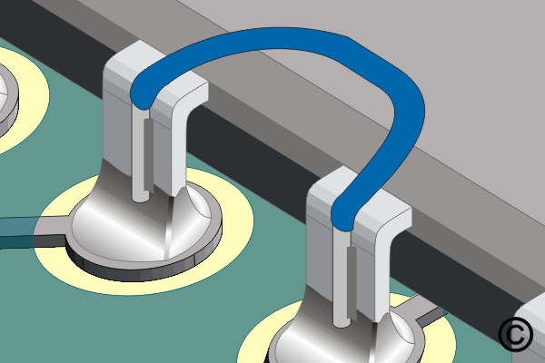
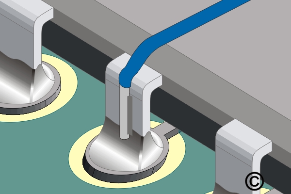
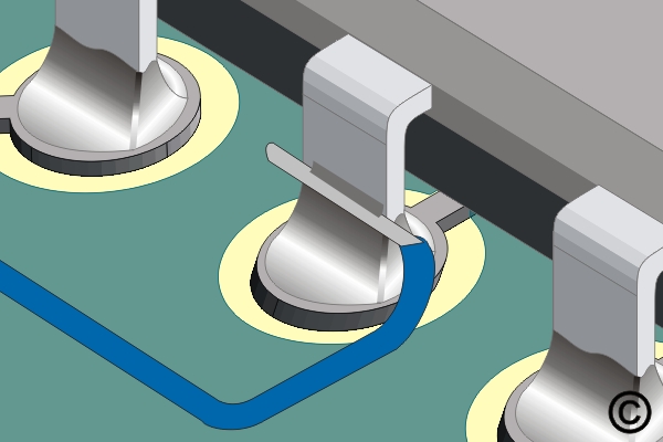
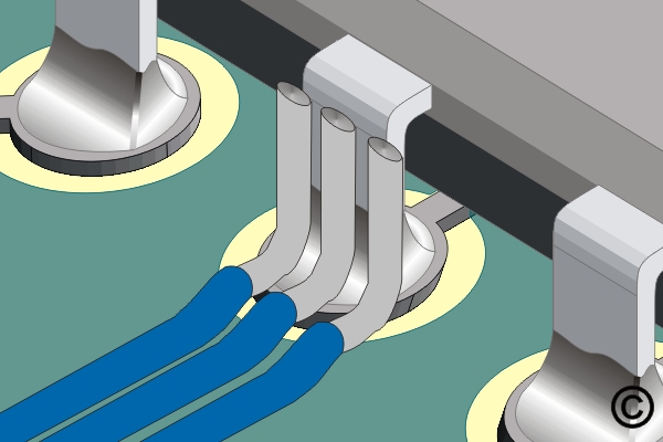
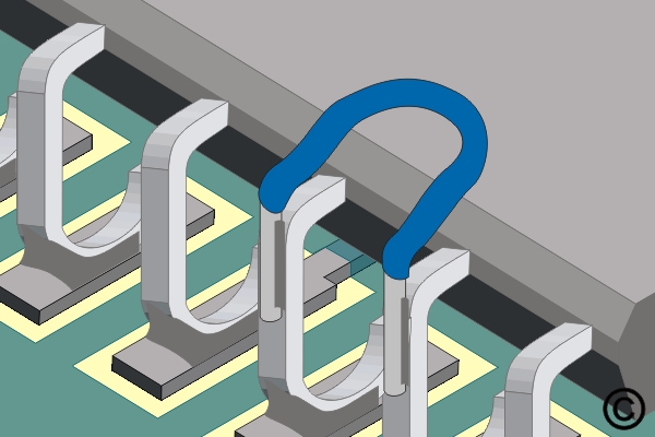
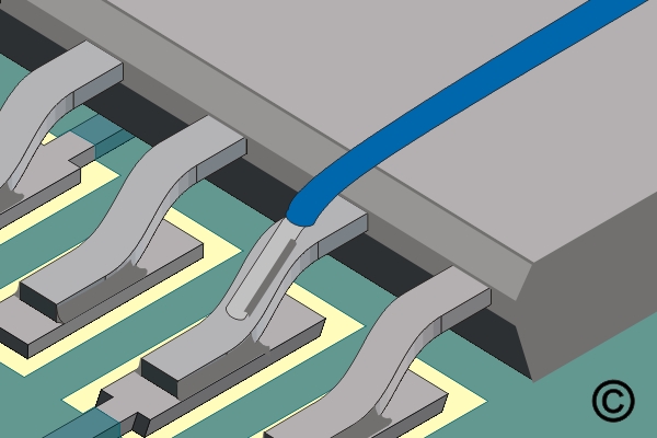
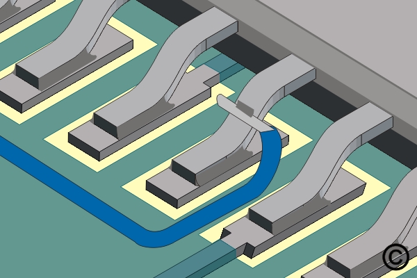
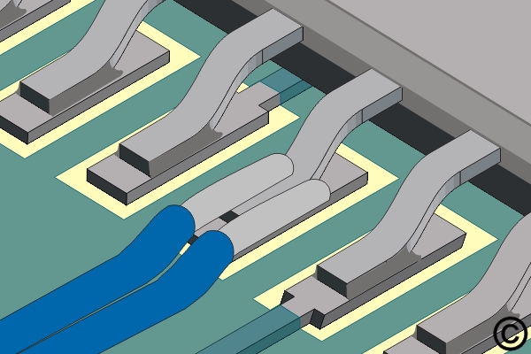
- Jumper wires shall be routed in an XY manner as directly as feasible, making as few bends as possible. (See Figure 1)
- Jumper wires shall not be raised more than 3.2 mm (.125") above the board surface or above components or leads in such a way that they will interfere with circuit board mounting.
- Bare conductor jumper wires longer than 12.7 mm (0.50") shall not be used. Bare conductor jumper wires shorter than 12.7 mm (0.50") shall not violate the minimum electrical clearance.
Note: The 12.7 mm (0.50") dimension refers to the length between terminations. - Jumper wires may pass over lands provided sufficient slack is available so that the wire can be moved away from the land for component replacement. Jumper wires shall not pass over pads or vias used as test points.
- Jumper wires shall not be routed under or over component leads or component bodies. Contact with heat sinks must be avoided.
- Jumper wires shall not pass through component footprints unless the layout of the assembly prohibits the routing in other areas.
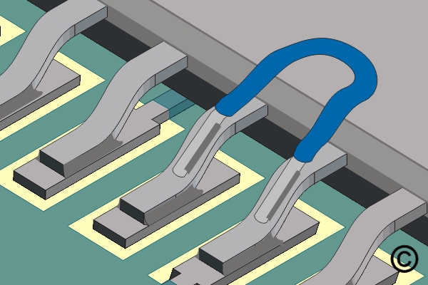
- Jumper wires shall have stress relief.
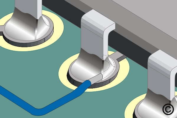
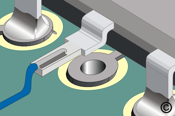
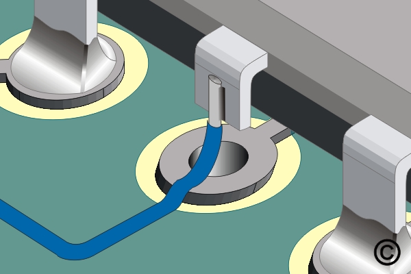
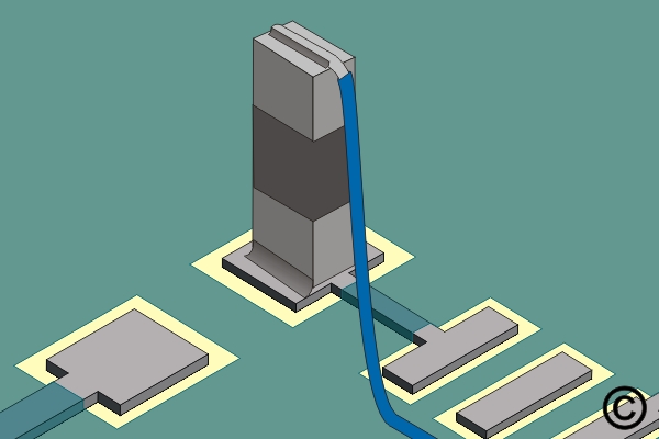
- Jumper wires may be routed through plated holes provided the wire is insulated, and insulation sleeving is placed in the hole. If a hole is needed, use the following method. (See Figure 2)
A. Drill a hole .25 mm (.010") larger than the insulation diameter.
B. Inspect the hole for burs or exposed internal circuits.
C. Document the added hole on a control drawing.
Note: Be careful that the drilled hole does not interfere with surface and internal conductors. - Jumper wires soldered into plated through holes must be discernible on the opposite side.
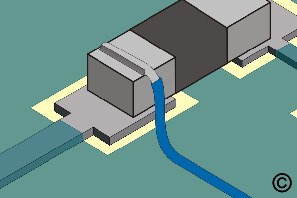
- Jumper wires soldered to lifted or clipped component leads may require insulation to prevent shorting. (See Figure 3)
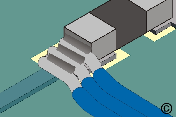
- Jumper wires may be terminated by a variety of methods. See illustrations.
PC Board Preparation
- Clean the area.
Note: When wires are in place, cleaning will often be more difficult. - Remove coating material or oxidation as necessary from the component leads, pads, or conductors where wire terminations will be soldered. Clean the area.
- Remove solder from the connection point if needed. Clean the area.
- Measure approximately the length of each wire needed.
Jumper Wire Selection
- Bare conductor jumper wires longer than 12.7 mm (0.50") shall not be used. Bare conductor jumper wires shorter than 12.7 mm (0.50") shall not violate the minimum electrical clearance.
Note: The 12.7 mm (0.50") dimension refers to the length between terminations. - Silver-plated wire must not be used; under some conditions, corrosion of the wire can occur.
- The smallest diameter wire that will carry the required current should be selected.
- Insulation requirements of the wire should withstand soldering temperatures, have some abrasion resistance, and have a dielectric resistance equal to or better than the board insulation material.
- Recommended wire is solid insulated copper wire, tin-lead plated, 22 to 32 AWG with Kynar, Milene, Kapton, Teflon, or equivalent insulation.
Caution: Wires with nicked or damaged conductors should not be used.
Jumper Wire Preparation
- Cut the jumper wires approximately 12.7 mm (0.50") longer than the estimated length needed.
Note: The length and gauge of the jumper wire may be critical. All wires have an electrical resistance (impedance) to the flow of electricity. This impedance is vital to electronic circuitry. Always refer to wiring lists for specific jumper wire requirements. - Strip insulation from each end of the jumper wire.
Note: Strip length is dependent on the termination style. - If required, tin the stripped ends with solder. Clean if necessary.
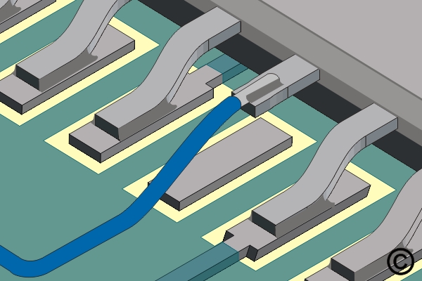
Jumper Wire Terminating and Routing
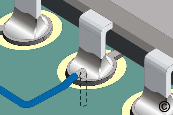
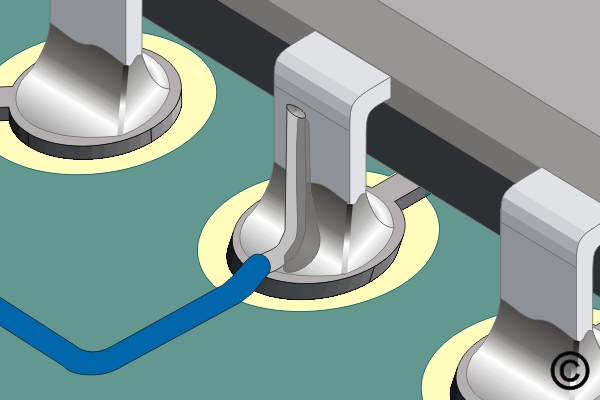
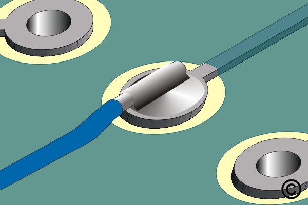
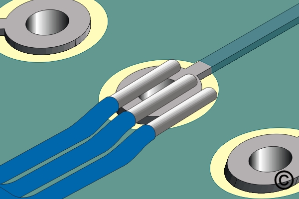
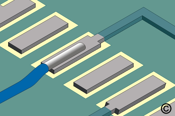
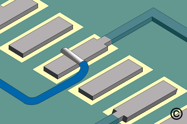
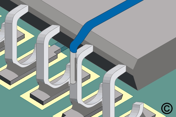
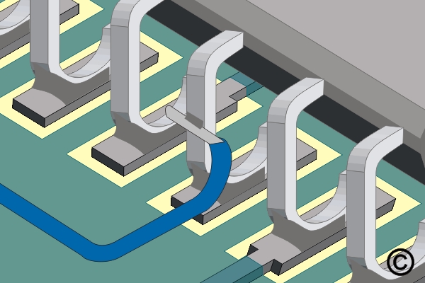
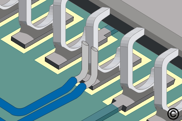
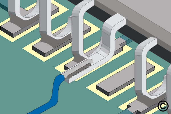
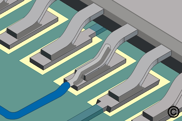
- Form the wire as needed and place the wire in position depending on the termination style. Center the wire on the component lead or pad; do not overhang the sides. If the wire is soldered to a pin, terminal, or component lead, wrap the wire a minimum of 90 degrees.
- Solder one end of the wire. Clean if necessary.
Note: Solder joint length must meet acceptability requirements.
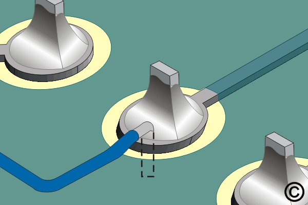
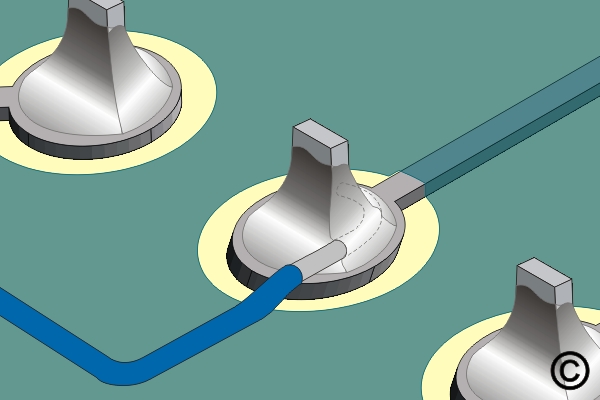
Caution: The insulation shall not be stripped back more than two wire diameters from the solder joint. Wire insulation may touch but not penetrate the solder joint, provided proper wetting of the wire is evident. - Bend the wire as needed and run the wire along the board surface. Route the jumper wire using the shortest route in an XY direction with the fewest possible bends to the second termination point.
Note: Jumper wires shall not be routed under or over component leads or component bodies. Contact with heat sinks must be avoided.
Caution: Do not bend the wire tighter than a radius of 3 times the conductor diameter. - After routing the jumper wire, solder the opposite end. Clean if necessary.
Caution: Wires soldered to lifted or clipped component leads may require insulation to prevent shorting.
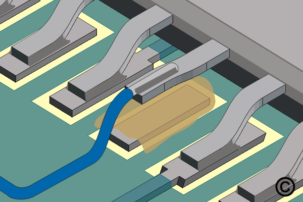
Jumper Wire Bonding
- After the wire has been soldered at both ends and cleaned if necessary, the wire should be bonded to the board surface.
Note: Bonding is not required if the wire is insulated and the insulated length is less than 25 mm - 1.00". - Bond the jumper wire using one of the following methods.
- Tape Dots or Tape Strips. (See Figure 4)
- Quick Set Adhesive. (See Figure 5)
- Hot Melt Adhesive. (See Figure 5)
- Hot Bonding. Some jumper wires are manufactured with a special thermo-set adhesive coating and are thermally bonded to the board surface with a special bonding tool. (See Figure 6)
- Bond the jumper wire within 6.0 mm (0.25") of each solder joint.
- Bond the jumper wire within 6.0 mm (0.25") of each bend in the wire.
- Bond the jumper wire at intervals not less than 25 mm (1.00") on straight runs.
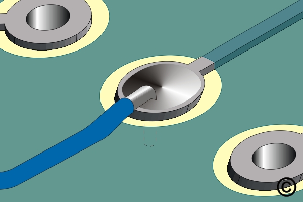
Jumper Wire Termination Figures - Through Hole Components
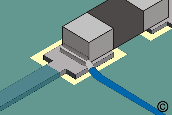
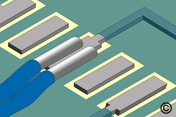
Jumper Wire Termination Figures - Chip Components, Pads and Conductors
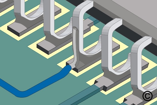
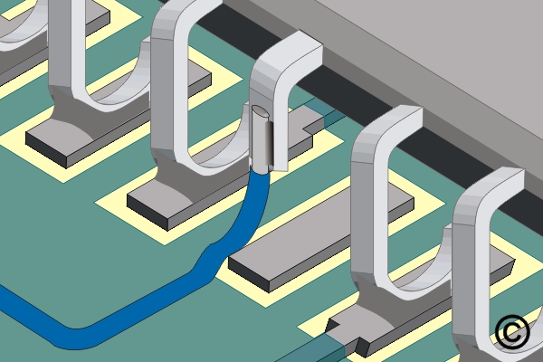
Jumper Wire Termination Figures - J-Lead Components
Jumper Wire Termination Figures - Gull Wing Components
Images
