Introduction
This paper provides a comprehensive overview of the challenges and best practices for the reballing of Ball Grid Array (BGA) components. The paper examines the complexities of removing and replacing solder balls on Ball Grid Arrays (BGAs), emphasizing the importance of achieving high-reliability connections. The guide covers various topics, including selecting appropriate reballing techniques, the importance of accurate alignment, considerations for solder ball composition, and the significance of proper thermal profiling.
Details
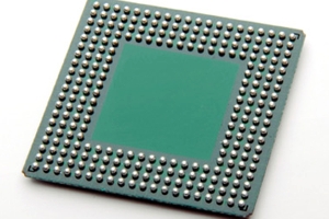
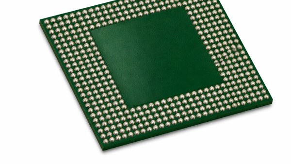
Some ball grid array (BGA) devices need to be converted from a lead-free finish, predominantly from a SAC305 (Sn96.5/Ag3.0/Cu0.5) to a tin-lead (Sn63Pb37) finish to meet the requirements of various defense, aerospace, or other high-reliability applications where the use of lead-free solder is not allowed due to tin whisker concerns.
The first step in this conversion process is deballing, in which the original lead-free solder balls are removed from the underside of the BGA device, exposing the interposer's pads. This deballing process is followed by either manual or automated reballing, which involves fluxing, aligning, and attaching new solder spheres of the replacement alloy, reflowing, inspecting, cleaning, performing any specified tests, and repackaging.
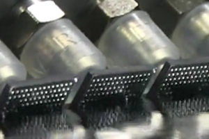
BGA deballing of SAC305 components is best accomplished using a robotic hot-solder-dip (RHSD) machine equipped with a dynamic solder wave and Sn63Pb37 solder. See image 2.
Robotic hot-solder dip machines are available with single- or dual-solder-wave options. A single-wave stripping process is adequate. The dynamic solder wave has sufficient scrubbing action to completely remove and replace the original SAC solder with a thin meniscus of Sn63/Pb37 solder. A dual solder wave for BGA de-balling is typically not recommended since the additional thermal cycle can degrade the BGA device. Any residual silver or copper from the original SAC305 interconnections would be negligible.
Even though SAC305 is predominantly tin, routine analysis of the stripping pot must be performed to ensure the silver contamination level remains below the J-STD-001 allowable maximum of 0.10% and the copper contamination level remains below 0.02%. If the alloy in the stripping pot becomes contaminated with lead-free solder, the remaining solder could also become contaminated.
Automated de-balling processing can be performed on multiple BGA devices using an RHSD machine equipped with a multiple-position arm and includes the following process steps:
- Automated vacuum pickup of multiple BGA components from a JEDEC matrix tray or custom-machined tray utilizing the multi-axis robotic system
- Flux application to existing BGA solder spheres
- Removal of excessive flux with an air knife
- Programmable pre-heat cycle to activate flux and pre-heat the BGA package
- Dynamic solder wave to remove and flush away original solder balls
- An ultra-filtered heated water rinse to remove flux residues
- Drying of BGA components with an air knife
- De-balled components returned to the matrix tray
- Clean and inspect BGA components
BGA component reballing services are available for BGA devices with a pitch as fine as 0.35 mm. There are various methods for solder sphere attachment during reballing BGAs and other area-array devices, such as land grid array (LGA) and quad flatpack (QFP) devices, as well as no-lead (QFN) devices. These methods include solder paste deposition and the use of tacky flux and replacement solder spheres. BGA component reballing services are available for BGA devices with a pitch as fine as 0.35 mm.
Ball count, device pitch, sphere diameter, solder alloy, and package size are all factors to consider when selecting the appropriate method. The use of tacky flux is the most common approach, as solder paste volume variability contributes to the final sphere volume variability. Therefore, the sphere size and the paste can create additional voiding by incorporating flux volatiles into the last sphere.
Following the de-ball process, re-ball of individual or multiple BGA devices is carried out, consisting of the following process steps:
- BGA components placed in custom fixtures
- Flux applied to BGA pads
- Precision aperture stencil positioned above the BGA device
- Fill apertures with solder spheres of the new alloy
- Solder sphere attachment is carried out with a multi-stage reflow oven or an IR oven
- Clean and inspect BGA components
- Bake as required to comply with MSL requirements
Post-reballing process inspection protocols should include the following:
- Z-height of solder balls to the bottom interposer surface, verifying device co-planarity
- Missing solder balls
- Solder ball volume
- Oversized solder ball volume
- Shorts between adjacent solder balls
- Detection of foreign object debris
When re-balling, the use of reliable, repeatable, and industry-wide proven processes that comply with the following are recommended or specified by customer specifications:
- J-STD-001 Requirements for Soldered Electrical and Electronic Assemblies
- GEIA-STD-0006 Requirements for Using Solder Dip to Replace the Finish on Electronic Piece Parts
- IEC TS 62647-4 Process Management for Avionics - Aerospace and Defense Electronic Systems
Post-ball verification and inspection services, at a minimum, will include a visual inspection at 10x magnification to confirm sphere condition, ball alignment, size, and location. Additional post-processing inspection and testing may be required on all or a sampling of parts, including:
- Ionic cleanliness (ROSE) testing per IPC-TM-650-2.3.25
- XRF for alloy composition and finish thickness per JESD 213
- X-ray inspection for solder ball void analysis per J-STD-001
- Solderability testing per J-STD-002
- SAM (scanning acoustic microscopy) testing per J-STD-035
- Ball shear testing per JESD22-B117
- Destructive physical analysis (DPA) per MIL-STD-1580
- Hermeticity testing (fine and gross leak) per MIL-STD-883
- Temperature, humidity, and bias testing
- Parametric testing
Upon completion of reballing, inspection, and testing, the re-marking of components may also be specified. There are various options for component marking, such as
- Epoxy ink dot marking per Mil-STD-130, Mil-STD-883, and or A-A-56032, and other standards-driven by customer requirements
- Laser marking with a revised part number
- Component labeling per Mil-STD-130, Mil-STD-883 and or A-A-56032, and other standards-driven by customer requirements
Finally, the re-balled devices can be re-packaged. Packaging considerations include:
- Tape and reel service per EIA-481
- Component MSL dry bake per J-STD-033
- Component MSL packaging in vacuum-sealed barrier bags with desiccant pack and moisture indicator card per J-STD-020
- Package identification and MSL labeling
Conclusions
This paper provides a comprehensive and insightful analysis of the critical issue of BGA component reballing. The authors' focus on the challenges and best practices associated with reballing techniques offers valuable guidance to engineers and technicians. The paper emphasizes the importance of high-reliability standards, such as proper inspection, cleaning, soldering, and reflow profiles, to ensure successful reballing of BGA components.
With its well-researched content and practical recommendations, this guide is an essential resource for professionals striving to achieve optimal performance and reliability in their BGA reballing processes.
Several members of the Circuit Technology Center team contributed to this technical paper. Images may be altered or recreated to protect proprietary information.