Sometimes, an error occurs at the most inopportune time; in this case, it was in the design phase of the printed circuit board. When circuit boards are in the prototype phase, it is not uncommon for sockets to be used at BGA sites. Design Engineers must lay out the BGA sites to meet the requirements of the selected test socket. Many of these sockets rely on a flat surface that precludes the use of a solder mask.
Eliminating solder masks is fine until it is time to move on with production, when BGA components will be soldered directly, eliminating the socket. You're probably not surprised that there is an occasional blunder at this point. In this case, the solder mask layer was omitted. Have you tried soldering a BGA component onto an unmasked BGA site?
The primary purpose of a solder mask at a BGA site is to isolate the area where solder wets, specifically the BGA pad. The solder mask isolates the pad from the conductor or the circuit, leading to a via or plated hole. Without the solder mask, the molten solder will bleed away onto the connecting pad or into the attached vias. Solder joint opens, and shorts are guaranteed.
The obvious key to preventing this would have been redesigning the circuit board and adding the mask layer. Since that was not done, solving the missing mask issue can be approached in a few ways.
Option One:
Scrap, a major ouch to the pocketbook.
Option Two:
Use the same socket that was used during the prototype phase. This may not be a practical solution, but it can be explored. BGA sockets tend to be expensive, and the durability of the connection can be a concern.
Option Three:
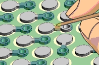
Rework the solder mask at the site. There are several ways to accomplish this. The most common method is to manually apply the solder mask or an equivalent high-temperature epoxy to the site. Before applying the mask, thoroughly clean the surface to remove any contaminants and ensure optimal adhesion of the mask to the surface.
Complete coverage of the site is not always necessary; the key is creating the isolation barrier, and this can sometimes be accomplished with a much smaller mask application at the connecting circuit while leaving the adjacent area clear.
This technique requires a steady hand and uses various tools, including a controlled dispensing system or fine-tipped probes, along with tape or a template to shield the solder mask from reaching undesired locations. This can be tedious and time-consuming, but it will get you the desired result.
Several members of the Circuit Technology Center team contributed to this feature story. Images may be altered or recreated to protect proprietary information.