Outline
This method is used to change a circuit path at a BGA site for engineering changes or modifications.
Note: This procedure requires precision milling equipment and highly trained technicians.
Caution: This procedure is not applicable for "via in pad" applications.
Minimum Skill Level - Expert
Recommended for technicians with advanced soldering and component rework skills and extensive experience in most repair/rework procedures.Conformance Level - Medium
This procedure may have some variance with the physical character of the original and most likely varies with some of the functional, environmental and serviceability factors.| Procedure References | |
| 1-0 | 1.0 Foreword |
| 2-1 | 2.1 Handling Electronic Assemblies |
| 2-2 | 2.2 Cleaning Procedures |
| 2-5 | 2.5 Baking and Preheating |
| 2-7 | 2.7 Epoxy Mixing and Handling |
| 9-0 | 9.0 BGA Component Rework and Reballing Procedures |
Tools and Materials

Delivers the optimal heat for curing adhesive bonding film. |

Bonding Tips used to bond adehesive backed Circuit Frames. |

Clear, superior strength epoxy in two-compartment plastic packages. |

Circuit Frames for surface mount pad, BGA pad and conductor repair. |

Copper conductors to repair circuit board damage including traces and conductors. |

General purpose cleaner for removing contamination. |

Designed for end cutting and hole boring. |

Sturdy rack for PCBs used for rework and positioning. |

High temperature polyimide tape discs, .50" diameter. |

A must-have tool for precise cutting, scraping and trimming. |

Precision microscope with stand and lighting for work and inspection. |

Use for precision milling of circuit board materials. |

General purpose oven for drying, baking and curing epoxies. |

Precision drill press for accuracy and controlled depth drilling. |

Nine precision-crafted tools for detailed circuit board work. |

Hardened stainless steel tip for scraping solder mask and removing defects. |

Properly maintained soldering iron and properly sized soldering iron tips. |

Multiple sizes and tip configurations of tweezers for various small parts handling needs. |

Nonabrasive, low-linting wipes for cleanup. |
Procedure
Procedure
- Clean the area.
- Remove the BGA component if installed, remove excess solder from the pads, and clean and inspect the site using standard BGA rework equipment.
- Cut the short conductor (dog bone) connecting the BGA pad to the connecting via using a Precision Drill System or milling machine and an appropriate size end mill. (See Figure 1)
- Remove the existing BGA pad. Apply heat from a soldering iron if needed. (See Figure 2)
- Use a milling machine to mill a shallow groove in the board surface from the BGA pad area to the perimeter of the BGA site. Tight spacing may restrict the width of the channel to 0.25 mm (.010") or less. Use a carbide end mill approximately 0.050 mm (.002") wider than the new connecting circuit. (See Figure 2)
- Bond a replacement BGA pad in place using a bonding iron. (See Procedure 4.7.3) The new BGA pad must have a tail that will align with the circuit track to be added next. (See Figure 3)
- Select a Circuit Track to match the width and thickness of the circuit to be replaced. Cut a length approximately as needed. The Circuit Track should overlap the BGA tail section a minimum of 2 times the circuit width.
- Gently abrade the top and bottom of the new Circuit Track with the buffer to remove any oxidation and clean.
Note: If needed, the ends of the Circuit Track may be tinned with solder before lap soldering in place. - Position this new Circuit Track along the milled groove. The Circuit Track should overlap the existing circuit a minimum of 2 times the circuit width. (See Figure 4)
- Apply a small amount of liquid flux to the overlap joint.
- Lap solder the Circuit Track to the BGA tail section using solder and a soldering iron. Make sure the new circuit is aligned correctly.
- Solder one end of a fine-gauge wire to the end of the extending circuit. The opposite end of the wire will be soldered later. (See Figure 5)
- Clean the area.
- Mix epoxy. If desired, add a color agent to the mixed epoxy to match the circuit board color.
- Coat the top and sides of the replaced circuit with epoxy. The epoxy bonds the new circuit to the base board material and insulates the circuit. (See Figure 5)
- Cure the epoxy per Procedure 2.7 Epoxy Mixing and Handling.
Caution: Some components may be sensitive to high temperatures. - Clean the board as required.
- Install new BGA per applicable procedures.
- Route and terminate the other end of the jumper wire.
Evaluation
- Visual examination for alignment and overlap of the new circuit.
- Visual examination of the epoxy coating for texture and color match.
- Electrical tests as applicable.
Images

Jumper Wires, BGA Components, Circuit Track Method
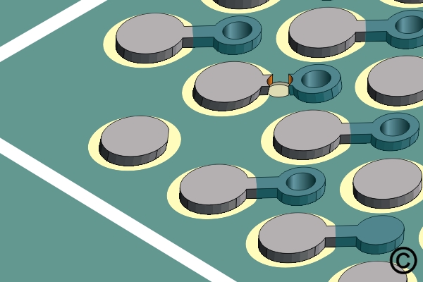
Cut the connection to the via using a Precision Drill System.
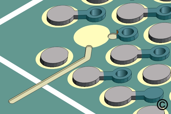
Remove the BGA pad and mill a shallow channel into the solder mask surface.
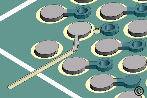
Bond a new BGA pad in place.
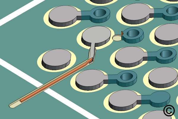
Solder a copper circuit track to the tail extending from the new BGA pad
Solder a wire to the Circuit Track and overcoat with epoxy.