What industry standard applies to a pad/part size mismatch?
Well, how's this for a mouthful, "IPC-J-STD-001D, Requirements for Soldered Electrical and Electronic Assemblies, Table 7-4, Dimensional Criteria- Chip Components - Rectangular or Square End Components - 1, 3 or 5."
In this case, it's specifically the minimum end solder joint width on a rectangular chip cap. Of course, that's not to mention "IPC-A-610D, 8.2.2.9 ..." Which basically deals with the same subject.
It's a wonder pad to part size mismatch doesn't happen more often, considering the thousands and thousands of opportunities on assemblies.
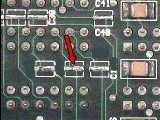
When it does happen, it's a big problem. Try as hard as possible to read a solution into the IPC specs; it's not always simple. In Figures 1 and 2, you can see the results of a part/pad mismatch.
Through the artwork design phase of this circuit board, there was an error in the pad layout. What should have been two individual pads for a 1206 chip component ended up being a single elongated pad.
If the pad were the proper width, the fix would have been relatively simple; create a small separation in the middle of the two ends. Unfortunately, the single pad was too narrow.
The applied class three criteria required a 75% end-width connection, and this component was a little too wide to satisfy that standard. "Bill Boarding," the component that is setting it on its side, was briefly considered as that would have allowed the component to meet the end width requirements, but the vulnerability of the components when placed at multiple locations was a matter of concern.
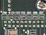
After multiple measurements, component placements, comparisons, and conversations, it was decided that these pads would not do as they were. Over thirty locations per board needed a fix.
What could be done? Replace the pads with the proper size pads! Not every assembly justifies this effort, but when it has the proper value and time is of the essence, it's worthwhile to proceed with this time-consuming rework.
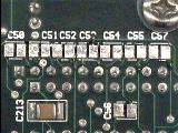
Our procedure 4.7.2 Surface Mount Pad Repair, Film Adhesive Method outlines the basic process for conducting this repair. The connecting conductors varied in this case, so many pads had to be cut to size.
It was quite a project to prepare and bond over 60 pads. Figure 3 shows a row of un-repaired pads. Figure 4 shows the same row with a new set of pads.
The customer was able to get the board up and functioning. Another case solved.