When a major OEM came to us with a design issue on fifty prototype circuit boards, the pressure was on. Two pairs of .005" wide traces had been routed with reversed polarity—and to complicate matters, they were buried deep within the board: one pair on layer 4, the other on layer 18. These were 18-layer, fully populated boards, and time was critical.
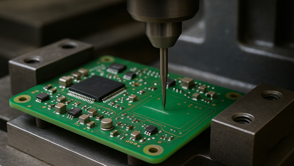
To locate and access the internal traces without damaging surrounding layers, we secured each board in a fixture and used a precision milling machine outfitted with a .050" carbide end mill. Guided by a stereo microscope and an X-ray system, our technicians carefully milled a slot just deep enough to expose the copper traces (Figures 1 and 2).
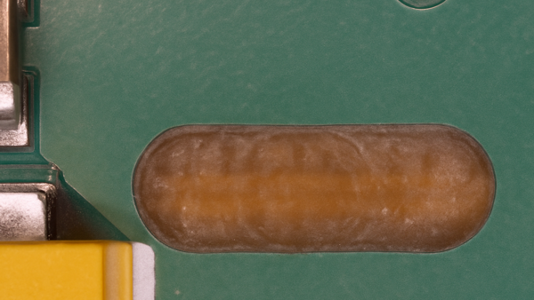
Next, using a specialized knife, we removed the remaining thin layer of base material by hand to reveal the copper. Each trace was precisely cut and tinned with solder. To correct the polarity issue, we tinned short copper ribbons and soldered them in place—crossing each pair accurately. For added protection, an approved insulating layer was placed over the first crossover before the second connection was completed.
To finish the job, each milled slot was filled with a high-strength epoxy, color-matched to blend seamlessly with the board. The result? A clean, precise, and functional repair that impressed the customer and met their critical production schedule.
This project showcased the skill, patience, and expertise of our technicians—and delivered a solution when it mattered most.
Several members of the Circuit Technology Center team contributed to this feature story. Images may be altered or recreated to protect proprietary information.