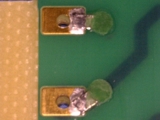
Several multilayer backplanes were mistakenly manufactured with missing plating for 24 holes on each board. The top and bottom side pads were in place, but the holes had no plating, so the inner layers were not connected.
Each hole required an internal connection to either layer 2 or layer 3. Making connections to various layers complicated the rework solution, and of course, these backplanes were critical, so a reliable rework method was required ASAP.
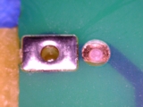
Due to ground shielding on the bottom side of the backplane, all rework needed to be completed from the top side. Figure 1 shows the top side of the board with a location that requires rework to establish missing internal connections. You can see the first step completed milling down to the internal layer.
After consultation with our engineers, our rework operators, and the customer, it was decided that the best rework approach would be as follows.
- Use a Precision Drill system fitted with a stereo microscope and a 0.080" carbide end mill, and carefully machine down to the respective internal layer to expose the copper signal trace. See Figure 1.
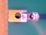
- Select a length of 2 oz. pure copper ribbon that matched the width of the signal trace.
- Tin the copper ribbon and the exposed inner layer with solder.
- Solder the copper ribbon from the exposed internal layer to the top side surface pad and electrically test to confirm the connection. See Figure 2.
- Complete the rework by filling each milled hole using color-matched high-strength 2-part epoxy and cure as required. See figure 3.
Several members of the Circuit Technology Center team contributed to this feature story. Images may be altered or recreated to protect proprietary information.