Outline
This method replaces damaged surface mount pads with new adhesive-backed dry film pads. The new pads are bonded to the circuit board surface using a bonding iron.
Caution: It is essential that the board surface be smooth and flat. If the base material is damaged, see the appropriate procedure.
Note: This method uses replacement surface mount pads. The new pads are fabricated from copper foil. They are available in many sizes and shapes and are generally supplied solder plated.
Minimum Skill Level - Advanced
Recommended for technicians with soldering and component rework skills and exposure to most repair/rework procedures, but lacking extensive experience.Conformance Level - High
This procedure most closely duplicates the physical characteristics of the original, and most probably complies with all the functional, environmental and serviceability factors.| Procedure References | |
| 1-0 | 1.0 Foreword |
| 2-1 | 2.1 Handling Electronic Assemblies |
| 2-2 | 2.2 Cleaning Procedures |
| 2-5 | 2.5 Baking and Preheating |
| 2-7 | 2.7 Epoxy Mixing and Handling |
Tools and Materials
|
Bonding Iron
Delivers the optimal heat for curing adhesive bonding film. |
|
Bonding Tips
Bonding Tips used to bond adehesive backed Circuit Frames. |
|
Circuit Bond Epoxy
Clear, superior strength epoxy in two-compartment plastic packages. |
|
Circuit Bonding System
System to repair damaged conductors, BGA pads, and SMT pads. |
|
Circuit Frames
Circuit Frames for surface mount pad, BGA pad and conductor repair. |
General purpose cleaner for removing contamination. |
|
Cleaning Brushes
Disposable brushes for solvent cleaning and application of coatings. |
|
Flex-Rack PCB Holder
Sturdy rack for PCBs used for rework and positioning. |
|
High Temp Tape Discs
High temperature polyimide tape discs, .50" diameter. |
|
Knife with #16 Blades
A must-have tool for precise cutting, scraping and trimming. |
Precision microscope with stand and lighting for work and inspection. |
General purpose oven for drying, baking and curing epoxies. |
|
Precision Tool Set
Nine precision-crafted tools for detailed circuit board work. |
|
Repair Skills Practice Kit
Training kit to practice circuit board repair skills prior to testing for certification. |
|
Scraper, Curved Tip
Hardened stainless steel tip for scraping solder mask and removing defects. |
Properly maintained soldering iron and properly sized soldering iron tips. |
Multiple sizes and tip configurations of tweezers for various small parts handling needs. |
Nonabrasive, low-linting wipes for cleanup. |
Procedure
- Clean the area.
- Remove the defective pad and a short length of the connecting circuit. (See Figure 1)
- Use a knife and scrape off any epoxy residue, contamination, or burned material from the board surface.
- Scrap any solder mask or coating from the connecting circuit. (See Figure 1)
- Clean the area.
- Apply a small amount of liquid flux to the connection area on the board surface and tin with solder. Clean the area. The length of the overlap solder connection should be a minimum of 2 times the circuit width.
- The area for the new pad on the board surface must be smooth and flat. If internal fibers of the board are exposed, or if there are deep scratches on the surface, they should be repaired. Refer to the appropriate procedure.
- Select a replacement surface mount pad that most closely matches the original surface mount pad. If a special size or shape is needed, they can be custom fabricated. (See Figure 2)
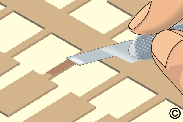
Note: New surface-mount pads are fabricated from copper foil. The foil is plated on the top with solder, and an adhesive bonding film is applied to the bottom. - Before trimming out the new pad, carefully scrape off the adhesive bonding film from the solder joint connection area on the back of the new pad. (See Figure 3)
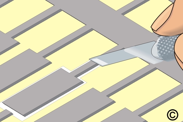
Caution: Scrape off the epoxy backing only from the joint connection area. Avoid touching the epoxy backing with your fingers or other materials that may contaminate the surface and reduce the bond strength when handling the replacement contact. - Cut out and trim the new pad. Cut out from the plated side. Cut the length to provide the maximum allowable circuit overlap for soldering. Minimum two times the circuit width. (See Figure 4)
- Place a piece of High-Temperature Tape over the top surface of the new pad. Place the new pad into position on the circuit board surface using the tape to help in alignment. (See Figure 5)
- Select a bonding tip with a shape to match the shape of the new pad. See the bonding tip chart in the replacement parts section of the manual provided with the repair system or repair kit.
Note: The tip used for bonding should be as small as possible, but should completely cover the entire surface of the new pad. - Position the circuit board so that it is flat and stable. Gently place the hot bonding tip onto the High-Temperature Tape covering the new pad. Apply pressure as recommended in the manual of the repair system or repair kit for 5 seconds to tack the new pad in place. Carefully peel off the tape.
Caution: Excessive bonding pressure may cause measling in the circuit board surface or may cause the new pad to slide out of position. - Gently place the bonding tip directly onto the new pad. Apply pressure as recommended in the manual of the repair system or repair kit for an additional 30 seconds to bond the pad fully. After the bonding cycle, the new pad is fully cured. Carefully clean the area and inspect the new pad for proper alignment.
- If the new pad has a connecting circuit apply a small amount of liquid flux to the lap solder joint connection area and solder the circuit from the new pad to the circuit on the circuit board surface. Use minimal flux and solder to ensure a reliable connection. Tape may be placed over the top of the new pad to prevent excess solder overflow.
Note: If the configuration permits, the overlap solder joint connection should be a minimum of 3.00 mm (0.125") from the related termination. This gap will minimize the possibility of simultaneous reflow during soldering operations. Refer to 7.1 Soldering Basics. - Mix epoxy and coat the lap solder joint connection. Cure the epoxy per Procedure 2.7 Epoxy Mixing and Handling.
Note: Additional epoxy can be applied around the perimeter of the new pad to provide additional bond strength.
Caution: Some components may be sensitive to high temperatures. - Apply surface coating to match prior coating as required.
Evaluation
- Visual examination.
- Measurement of new pad width and spacing.
- Electrical continuity measurement.
Images
Surface Mount Pad Repair, Film Adhesive Method
Remove the defective pad and remove soldermask from the connecting circuit.
Select a replacement pad that matches the missing pad.
Scrape off the adhesive bonding film from the solder joint area on the back of new pad.
Cut out the new surface mount pad. Cut from the plated side.
Place the new surface mount pad in place using Kapton tape.
Completed repair.