In every industry, there is a gap between conception and execution. It doesn't take long in this business to learn that ideas are essential, but they're usually the easiest part of the process. Putting a worthwhile idea into action can be exciting, challenging, and humbling. One of our customers found a small but critical error to their dismay.
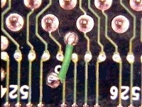
The ground plane, which should have served as a signal return path, was missing between plated through holes in a section of their circuit board. Thousands of boards were in the assembly pipeline and thousands in the field when a subtle disruption in the electronic operation of the final product became clear to the customer. As a result, they discovered the assembly would not operate properly. See Figure 1.
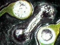
This problem occurred between pads on a long row of closely spaced, plated-through holes. Fortunately, after testing several different rework options, the customer was able to correct the fault using a short jumper wire. However, after considering the use of wires, the end customer would not accept it. See Figure 2.
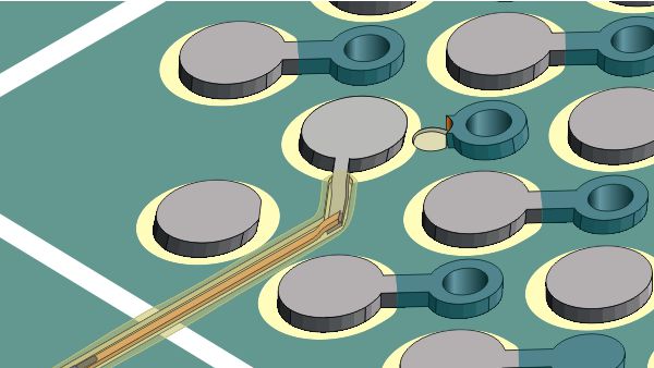
Was there a way to rework these boards without the obvious surface wires being visible? We reviewed the possibilities and developed a reliable and repeatable process. Here it is. The first step was to mill down to the layer requiring the connection. This was accomplished by a skilled operator using a precision, depth-controlled milling machine. The inner layer of copper was exposed; a delicate operation.
Additionally, a shallow groove was machined into the circuit board surface to allow the new conductor routing to remain below the surface. The next step was an exercise in fine motor dexterity. Our technician soldered new conductors across the gap.
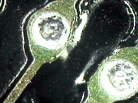
The tools and materials used included a microscope, solder, a fine-tipped soldering iron, and copper foil conductor, .008" wide. See Figure 3. At this point, the circuit boards were sent for inspection to ensure that the solder joints and routing followed the specifications.
After inspection, the boards were returned to the technicians, who filled the machined groove with high-temperature, thermo-setting epoxy. The epoxy was blended into the board's surface using a coloring agent. The results are presented in Figure 4 below.
The repair was performed at 8 locations on each circuit board. It was performed reliably and economically, bridging the gap between conception and execution. On to the next project!
Several members of the Circuit Technology Center team contributed to this feature story. Images may be altered or recreated to protect proprietary information.