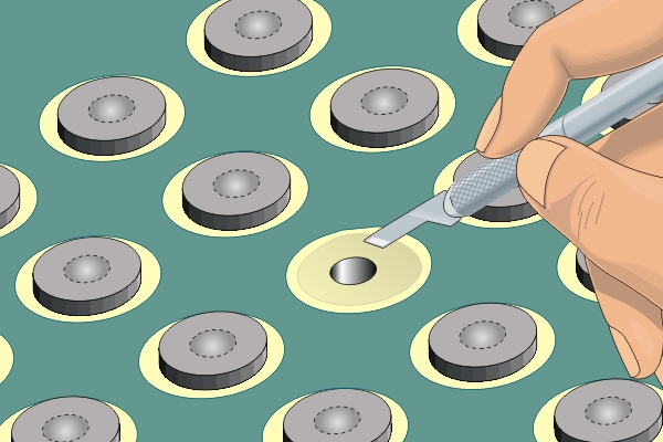
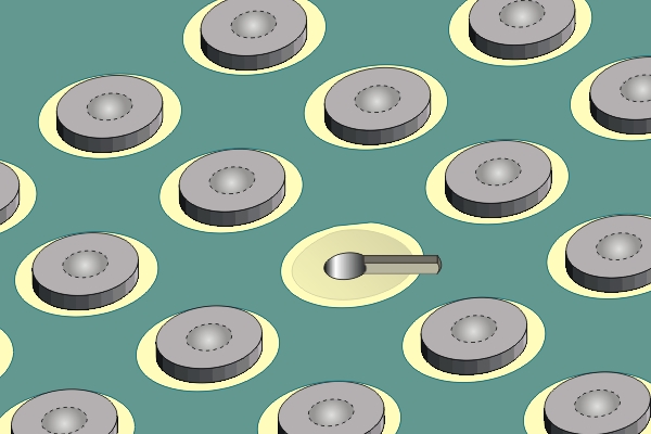
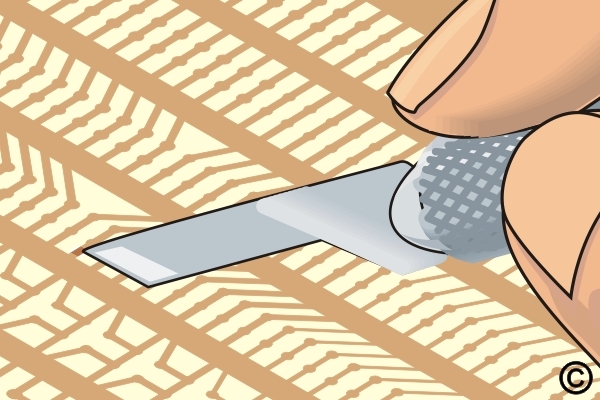
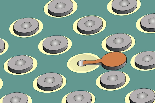
Circuit Technology Center
SEARCH  

4.7.4 Surface Mount, BGA Pad with Integral Via Repair

 
Outline
This method is used to replace damaged BGA pads with new dry film adhesive-backed pads. The new pads are bonded to the circuit board surface using a specially designed Bonding Iron. The electrical connection is made to a via which is originally manufactured integral to the pad.

Note: This method uses replacement BGA pads. The new pads are fabricated from copper foil. They are available in a variety of sizes and shapes and are generally supplied solder plated. If a special size or shape is needed, they can be custom fabricated.

Minimum Skill Level - Expert
Recommended for technicians with advanced soldering and component rework skills and extensive experience in most repair/rework procedures.

Conformance Level - Medium
This procedure may have some variance with the physical character of the original and most likely varies with some of the functional, environmental and serviceability factors.

Acceptability References
IPC-A-600 2.0 Externally Observable Characteristics
IPC-A-610 10.0 Laminate Conditions
Procedure References
1.0 Foreword
2.1 Handling Electronic Assemblies
2.2 Cleaning
2.5 Baking And Preheating
2.7 Epoxy Mixing and Handling
IPC7721 4.7.4 Surface Mount, BGA Land with Integral Via Repair Film Adhesive Method
Tools and Materials
115-3210
Bonding Iron, 120 VAC
Delivers the optimal heat for curing adhesive bonding film.
CircuitMedic Part
Circuit Frames
Circuit Frames
Cleaner
Cleaner
General purpose cleaner for removing contamination.
115-3302
Circuit Bond Epoxy
Clear, superior strength epoxy in two-compartment plastic packages.
235-3050
High Temp Tape Discs
High temperature polyimide tape discs, .50" diameter.
355-0614
Knife with #16 Blades
A must-have tool for precise cutting, scraping and trimming.
Microscope
Microscope
Precision microscope with stand and lighting for work and inspection.
Oven
Oven
General purpose oven for drying, baking and curing epoxies.
335-3197
Scraper
Hardened stainless steel tip for scraping solder mask and removing defects.
Solderinmg Iron
Soldering Iron
Properly maintained soldering iron and properly sized soldering iron tips.
Hot Plate
Tweezers
Multiple sizes and tip configurations of tweezers for various small parts handling needs.
Wipes
Wipes
Nonabrasive, low-linting wipes for cleanup.
Images and Figures
4.7.4 Surface Mount, BGA Pad with Integral Via Repair
Damaged BGA Pad
4.7.4 Surface Mount, BGA Pad with Integral Via Repair
Figure 1: Remove the defective pad and prepare connecting via.
4.7.4 Surface Mount, BGA Pad with Integral Via Repair
Figure 2: Mill or cut a shallow gully into the board surface from the via location to the outside edge of the affected pad.

4.7.4 Surface Mount, BGA Pad with Integral Via Repair
Figure 3: Select a replacement pad that matches the missing pad.
4.7.4 Surface Mount, BGA Pad with Integral Via Repair
Figure 4: Scrape off the adhesive bonding film from the solder joint connection area on the back of new pad.
4.7.4 Surface Mount, BGA Pad with Integral Via Repair
Figure 5: Connecting circuit is fit into via.

4.7.4 Surface Mount, BGA Pad with Integral Via Repair
Figure 6: Bond the new pad using a Bonding Iron.
4.7.4 Surface Mount, BGA Pad with Integral Via Repair
Figure 7: Completed repair.
Procedure
  1. Clean the area.
  2. Carefully remove the defective pad to avoid damaging the integral via.
  3. Use a knife and scrape off any epoxy residue, contamination, or burned material from the board surface.
  4. Scrape off any residue from the exposed via. (See Figure 1)
  5. Clean the area.
  6. Apply a small amount of liquid flux to the via connection on the board surface. Using the appropriate size solder braid, remove solder from the via. Clean the area.
  7. In general, the area for the new pad on the board surface must be smooth and flat. If internal fibers of the board are exposed, or if there are deep scratches on the surface, they should be repaired. Refer to the appropriate procedure. In this procedure, a trough or gully must be recessed into the board from the via location to the outside edge of the affected pad. This permits the via-to-pad connecting circuit adequate space for routing without interfering with the pressing of the new BGA pad. (See Figure 2)
  8. Select a replacement BGA pad that most closely matches the surface mount pad to be replaced. If a special size or shape is needed, they can be custom fabricated. (See Figure 3)
    Note: New BGA pads are fabricated from copper foil. The foil is plated on the top side with solder, and an adhesive bonding film is applied to the bottom side.
  9. Before trimming out the new pad, carefully scrape off the adhesive bonding film from the solder joint connection area on the back of the new pad. In order to ensure that the final pressed pad lays flat, it may be necessary to remove the film from the whole length of the connecting circuit up to the pad itself. (See Figure 4)
    Caution: When handling the replacement pad, avoid touching the epoxy backing with your fingers or other materials that may contaminate the surface and reduce the bond strength.
  10. Cut out and trim the new pad. Cut out from the plated side.
  11. Turning the pad upside down, place the pad on the board so that the connecting circuit can be fit into the via. Ensure the connecting circuit is running over the previously cut trough. (See Figure 5) The connecting circuit of the new BGA pad will be inserted into the integral via hole of the original BGA pad.
  12. Insert the connecting circuit into the via and carefully flux the connection area.
  13. Solder the connecting circuit into the via.
  14. Lay the connecting circuit into the bottom of the trough. If required, apply a securing film of high-strength epoxy over the connecting circuit to secure it in place and provide a flat surface on which to press the new BGA pad.
  15. Fold over the new BGA pad 180 degrees and place the new pad into position on the circuit board surface using high-temperature tape to help in alignment
  16. Select a bonding tip with a shape to match the shape of the new pad. See the bonding tip chart in the replacement parts section of the manual provided with the repair system or repair kit. (See Figure 6)
    Note: The tip used for bonding should be as small as possible but should completely cover the entire surface of the new pad.
  17. Position the circuit board so that it is flat and stable. Gently place the hot bonding tip onto the High-Temperature Tape covering the new pad. Apply pressure as recommended in the manual of the repair system or repair kit for 5 seconds to tack the new pad in place. Carefully peel off the tape.
    Caution: Excessive bonding pressure may cause measling in the circuit board surface or may cause the new pad to slide out of position.
  18. Gently place the bonding tip directly onto the new pad. Apply pressure as recommended in the manual of the repair system or repair kit for an additional 30 seconds to fully bond the pad. After the bonding cycle, remove the tape used for alignment. The new pad is fully cured. Carefully clean the area and inspect the new pad for proper alignment. (See Figure 7)
  19. Additional epoxy can be applied around the perimeter of the new pad to provide additional bond strength. Mix epoxy. Cure the epoxy per Procedure 2.7 Epoxy Mixing and Handling. Use the maximum recommended heat cycle to ensure the highest strength bond. BGA pads are routinely subjected to one or more reflow cycles.
    Caution: Some components may be sensitive to high temperatures.
  20. Apply surface coating to match prior coating as required.
Evaluation
  1. Visual examination.
  2. Measurement of new pad width and spacing.
  3. Electrical continuity measurement.
Procedure for reference only.