Circuit Technology Center 22 Parkridge Road
Haverhill, MA 01835 USA
www.circuitrework.com

4.7.1 Surface Mount Pad Repair, Epoxy Method

Repair damaged surface mount pads using epoxy-bonded replacement patterns. Includes pad alignment, bonding and finishing practices to restore solderable surfaces.


REQUEST FOR QUOTE    GUIDES INDEX
slide 1
Surface Mount Pad Repair, Epoxy Method
slide 2
Remove the defective pad and remove soldermask from the connecting circuit.
slide 3
Select a replacement pad that matches the missing pad.
slide 4
Cut out the new surface mount pad.
slide 5
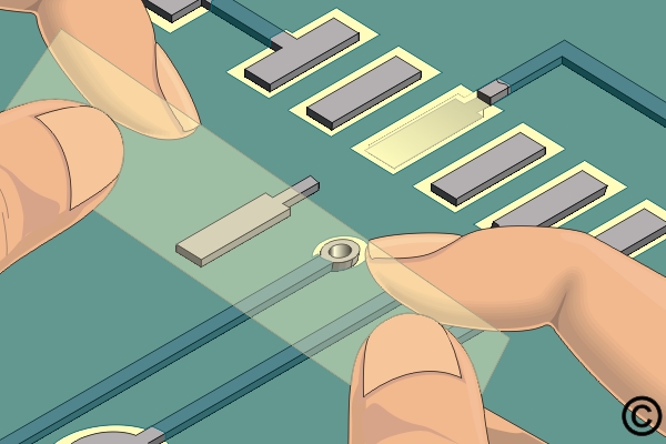
Place the new surface mount pad in place using high temperature tape.
slide 6
Completed repair.
SLIDESHOW STARTING

Outline

This method replaces damaged surface mount pads with commercially available replacement pads. The new pads are bonded to the circuit board surface using liquid epoxy.

Caution: The board surface must be smooth and flat. If the base material is damaged, follow the appropriate procedure.

Note: This method uses commercially available replacement surface mount pads. The new pads are fabricated from copper foil. They are available in hundreds of sizes and shapes and are generally supplied solder plated. If a special size or shape is needed, it can be custom-fabricated.

Minimum Skill Level - Advanced

Recommended for technicians with soldering and component rework skills and exposure to most repair/rework procedures, but lacking extensive experience.

Conformance Level - Medium

This procedure may have some variance with the physical character of the original and most likely varies with some of the functional, environmental and serviceability factors.

Tools and Materials

Procedure

  1. Clean the area.
  2. Remove the defective pad and a short length of the connecting circuit. (See Figure 1)
  3. Use a knife and scrape off any epoxy residue, contamination, or burned material from the board surface.
    Caution: Abrasion operations can generate electrostatic charges.
  4. Scrape off any solder mask or coating from the connecting circuit. (See Figure 1)
  5. Clean the area.
  6. Apply a small amount of liquid flux to the connection area on the board surface and tin with solder. Clean the area. The length of the overlap solder connection should be a minimum of 2 times the circuit width.
  7. The area for the new pad on the board surface must be smooth and flat. If the board's internal fibers are exposed or there are deep scratches on the surface, they should be repaired. Refer to the appropriate procedure.
  8. Select a commercially available surface mount pad that most closely matches the surface mount pad to be replaced. If a special size or shape is needed, it can be custom-fabricated. (See Figure 2)
  9. Cut out and trim the new pad. Cut the length to provide the maximum allowable circuit overlap for soldering. Minimum two times the circuit width. (See Figure 3)
    Note: The new replacement surface mount pad may be trimmed from a copper sheet.
  10. Mix the epoxy and apply a small amount to the surface where the new pad will be placed.
  11. Place a piece of High-Temperature Tape over the top surface of the new pad. Place the new pad into position on the circuit board surface using the tape to help in alignment. (See Figure 4)
  12. Cure the epoxy per Procedure 2.7 Epoxy Mixing and Handling.
    Caution: Some components may be sensitive to high temperatures.
  13. After the epoxy has cured, remove the tape used for alignment. Carefully clean the area and inspect the new pad for proper alignment.
  14. If the new pad has a connecting circuit, apply a small amount of liquid flux to the lap solder joint connection area and solder the circuit from the new pad to the circuit on the circuit board surface. Use minimal flux and solder to ensure a reliable connection. High-temperature Tape may be placed over the top of the new pad to prevent excess solder overflow.
    Note: If the configuration permits, the overlap solder joint connection should be a minimum of 3.00 mm (0.125") from the related termination. This gap will minimize the possibility of simultaneous reflow during soldering operations. Refer to 7.1 Soldering Basics.
  15. Mix epoxy and coat the lap solder joint connections. Cure the epoxy per the manufacturer's recommended instructions.
    Note: Additional epoxy can be applied around the perimeter of the new pad to provide additional bond strength.
  16. Apply surface coating to match the prior coating as required.

Evaluation

  1. Visual examination
  2. Measurement of new pad width and spacing.
  3. Electrical continuity measurement.

Images

QUICK QUESTION?
Have a general inquiry?
Send us a message below.
NEED A FORMAL QUOTE?
Submit a request using our quote form.