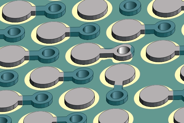
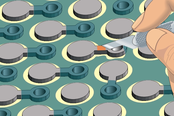
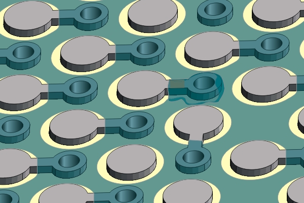
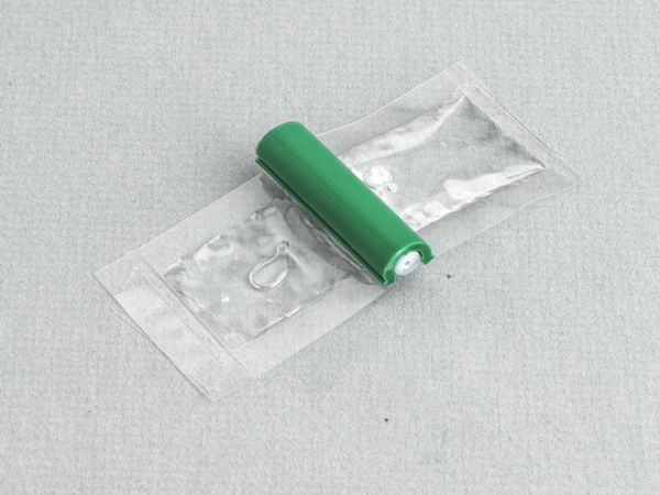
2.4.3 Coating Replacement, Solder Mask, BGA Locations
Restore solder mask in BGA locations while maintaining pad geometry and spacing. Detailed procedures ensure insulation integrity and reliable component reinstallation in high-density areas.
Minimum Skill Level: Intermediate
Conformance Level: High
REQUEST FOR QUOTE GUIDES INDEX