Outline
This method is used to repair damaged circuit surface planes. The damaged areas are repaired with dry film epoxy, adhesive-backed copper foil disks. They are bonded to the circuit board surface using a bonding press or bonding iron.
Caution: It is essential that the board surface be extremely smooth and flat. If the baseboard is damaged, see the appropriate procedure.
Minimum Skill Level - Advanced
Recommended for technicians with soldering and component rework skills and exposure to most repair/rework procedures, but lacking extensive experience.Conformance Level - High
This procedure most closely duplicates the physical characteristics of the original, and most probably complies with all the functional, environmental and serviceability factors.| Procedure References | |
| 1-0 | 1.0 Foreword |
| 2-1 | 2.1 Handling Electronic Assemblies |
| 2-2 | 2.2 Cleaning Procedures |
Tools and Materials

Mild abrasive for removing oxides and contaminants. |

Ball mills, abrasives and cutting tools for working on circuit boards. |

Delivers the optimal heat for curing adhesive bonding film. |

Bonding Tips used to bond adehesive backed Circuit Frames. |

Clear, superior strength epoxy in two-compartment plastic packages. |

System to repair damaged conductors, BGA pads, and SMT pads. |

Circuit Frames for surface mount pad, BGA pad and conductor repair. |

General purpose cleaner for removing contamination. |

Disposable brushes for solvent cleaning and application of coatings. |

Woven copper wire designed to wick solder from surfaces and holes. |

Designed for end cutting and hole boring. |

Sturdy rack for PCBs used for rework and positioning. |

High temperature polyimide tape discs, .50" diameter. |

A must-have tool for precise cutting, scraping and trimming. |

Precision microscope with stand and lighting for work and inspection. |

Use for precision milling of circuit board materials. |

General purpose oven for drying, baking and curing epoxies. |

Precision drill press for accuracy and controlled depth drilling. |

Nine precision-crafted tools for detailed circuit board work. |

Hardened stainless steel tip for scraping solder mask and removing defects. |

Properly maintained soldering iron and properly sized soldering iron tips. |

Multiple sizes and tip configurations of tweezers for various small parts handling needs. |
Procedure
Procedure
- Clean the area.
- Secure the circuit to a Precision Drill/Milling System with a microscope available for viewing. Use an end mill slightly larger than the void in the surface plane and make a counterbore through the surface plane only. Do not mill into the laminate material; you may expose inner-layer circuits.
Note: Several adjacent counterbores may be required to fill larger areas. - Clean the area with solvent.
- The area for the new Adhesive Backed Disk on the board surface must be smooth and flat. If internal fibers of the board are exposed or there are deep scratches on the surface, they should be repaired. Refer to the appropriate procedure.
- Select a replacement adhesive-backed disk that matches the size of the end mill used to make the counterbore.
Note: The thickness should be selected to meet the requirements of the circuit board surface plane thickness. - With the adhesive-backed disk positioned film side up, carefully scrape off the adhesive film from the outer 0.005" of the disk diameter.
- Position the adhesive-backed disk, film side down. Place a piece of High-Temperature Tape over the adhesive-backed disk, and position the adhesive-backed disk into the counterbore. Press the adhesive-backed disk into position. (See Figure 2)
- Select a bonding tip with a shape to match the shape of the adhesive-backed disk.
Note: The bonding tip should be as small as possible but should completely cover the entire surface of the adhesive-backed disk. - Position the circuit board so that it is flat and stable. Gently place the hot bonding tip onto the tape covering the adhesive-backed disk. Apply pressure and heat as recommended in the manual of the Repair System or Repair Kit for 5 seconds to tack the adhesive-backed disk in place. Carefully peel off the tape. (See Figure 2)
- Gently place the hot bonding tip directly onto the new adhesive-backed disk. Apply pressure and heat as recommended in the manual of the Repair System or Repair Kit for an additional 30 seconds to fully bond the new adhesive-backed disk. The new adhesive-backed disk is fully cured. Carefully clean the area and inspect the new adhesive-backed disk for alignment.
Note: Several adjacent counterbores may be required to fill larger areas. - Using flux and solder, carefully add a small amount of solder to a soldering iron with a "Blade" shaped tip, and flow solder over the repaired area.
- Using the "Blade" shaped soldering tip and desolder braid, remove any excess solder.
- Clean the area.
- Using the Electric/Hand Eraser, clean and buff the soldered area to blend the repair to the circuit surface.
- Using High-Temperature Tape, mask off an area larger than the repaired area.
- Using the abrasive pad, "lightly" buff the masked area to blend the repair to the circuit surface as necessary.
- Clean the area.
Final Finish
- Blend the surface type using an appropriate buffing material or abrasive pad.
- Matte and semi-gloss surfaces may require light abrasion to blend with the original surface finish type. High gloss will require polishing.
- Remove any loose particles as necessary and clean the area.
Evaluation
- Visual examination.
- Electrical tests as applicable.
Images

Conductor Repair, Surface Plane, Film Adhesive Method
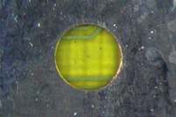
Milled area showing removal of damaged surface conductor foil.

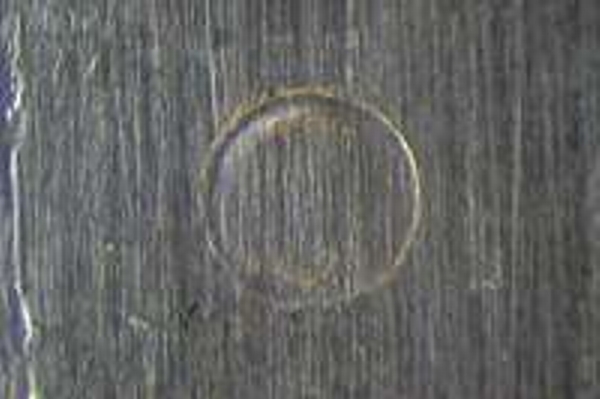
The transplant conductor foil in place.
The transplant conductor foil bonded, soldered and blended to the surrounding surface.