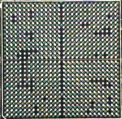
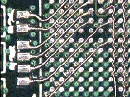
This redesign project centered around a 676-ball BGA (Ball Grid Array) component. During evaluation, it was determined that 23 solder balls were not correctly connected (Figure 1).
The only feasible corrective action involved re-routing - an extensive redesign effort in any context. Re-routing would have been simplified if the affected pads were located along the perimeter of the BGA footprint; however, most of the problematic pads originated near the package center.
Re-Routing Strategy
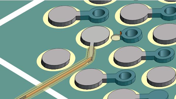
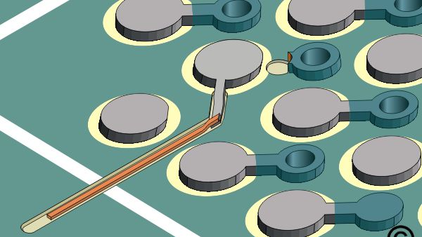
To accommodate the new connections, ribbon traces were extended outward from the inner BGA pads to the periphery of the component footprint. This approach allowed for making signal trace changes using wires beyond the perimeter of the component.
While straightforward conceptually, execution demanded precision. The design team first verified the corrected trace assignments. Next, the layout team translated these assignments into a usable physical layout (Figure 2).
Layout Considerations
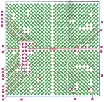
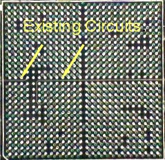
Initial point-to-point documentation provided a framework, but conflicts emerged when the design was adapted to the physical board. Existing surface conductors and pads constrained available routing paths (Figure 3).
Board Modification
To establish safe routing channels, technicians selectively removed solder mask using a precision high-speed drill (Figure 4). This process cleared the necessary pathways for conductor placement.
The original BGA pads were isolated from their vias and removed. New pads were bonded to the board surface in alignment with the re-routed conductors to ensure proper electrical orientation.
Conductor Installation
Following IPC Procedure 4.2.1, Conductor Repair, Foil Jumper, Epoxy Method, new copper traces were routed outward from the BGA footprint to perimeter pads. Each trace required careful shaping to accommodate bends and spacing constraints while maintaining the appropriate thickness and height profile to avoid interference during solder paste stenciling and final BGA placement.
The repair concluded with the placement of new SMT pads directly aligned to the extended conductors.
Conclusion
This re-routing project highlights the high level of precision required in advanced BGA rework. Successful execution demanded multidisciplinary collaboration - from design engineers to technicians performing delicate solder mask excavation and foil jumper installation. The final result demonstrates that even complex BGA modifications can be addressed through controlled, standards-based repair and rework methods.
Several members of the Circuit Technology Center team contributed to this feature story. Images may be altered or recreated to protect proprietary information.