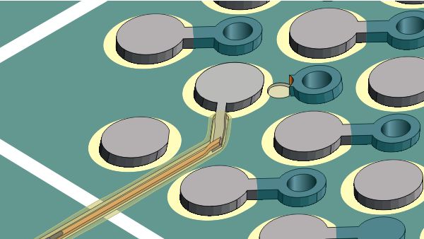
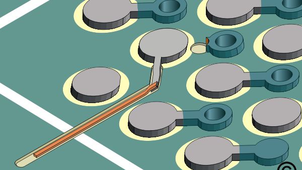
When circuit modifications are needed beneath a Ball Grid Array (BGA) component, traditional jumper wires are not practical due to space constraints. Circuit Technology Center provides a proven, precision solution using ultra-thin flat copper ribbon conductors. This low-profile method enables reliable modifications between the PCB surface and BGA underside without compromising electrical or mechanical performance. Performed by IPC-certified technicians with decades of experience, this process delivers consistent, high-reliability results. Our advanced BGA site modification services are trusted for critical applications where precision and performance are essential.
Key Highlights- Proprietary process using ultra-thin flat copper ribbons
- Reliable solution for modifications under BGA components
- Maintains mechanical and electrical integrity in tight spaces
- IPC-certified technicians with decades of rework experience
- Proven, time-tested technique trusted in critical applications
- Scalable service for prototype and production requirements
- Consistent results backed by rigorous process control
- Low-profile copper ribbon conductors for BGA site modifications
- Designed for use between PCB surface and BGA underside
- Eliminates limitations of traditional jumper wire methods
- Provides reliable connectivity without compromising PCB integrity
- Performed by IPC-certified technicians using documented procedures
- Suitable for high-reliability aerospace, defense, and advanced electronics applications
- 6.2.1 Jumper Wires, BGA Components, Circuit Track Method
- 6.2.2 Jumper Wires, BGA Components, Through-Board Method
- 9.0 BGA Component Rework and Reballing Procedures
- IPC 7711/7721 Rework, Modification, and Repair of Electronic Assemblies
- IPC-A-610 Acceptability of Electronic Assemblies
- IPC-A-620 Requirements and Acceptance for Cable and Wire Harness Assemblies
- IPC-J-STD-001 Requirements for Soldered Electrical and Electronic Assemblies
- IPC-JEDEC-J-STD-020 Moisture/Reflow Sensitivity Classification for Nonhermetic Surface Mount Devices
- IPC-JEDEC-J-STD-033 Handling, Packing, Shipping and Use of Moisture, Reflow, and Process Sensitive Devices
- IPC-7095 Design and Assembly Process Implementation for BGAs
- JESD625C.01 Requirements for Handling Electrostatic-Discharge-Sensitive (ESDS) Devices


