Rework for Missing Ground Connections
[unknown placeholder $article.blog_tech_summary$]
REQUEST FOR QUOTE BLOGS INDEX

|
|
22 Parkridge Road Haverhill, MA 01835 USA www.circuitrework.com |
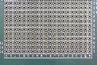
This latest problem is a board fabricated, as shown in Figure 1.
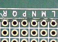
It is unclear in the photo, but plated holes A through V in Row 1 should have been connected to the ground to perform their function properly. They were not connected to each other or ground.
It would seem easy to find a ground point and connect the pins using a wire once the board was populated, but a surface wire was unacceptable.
A connection was needed at the bare board level. This new connection needed to be reliable without impacting the plated-through holes. The full row of plated holes needed to be connected to ground on layer 3.
Here Is The Solution
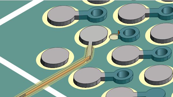
Using a precision milling system, we milled a groove directly adjacent to the row of pads. Under high magnification, we cleared a small space under the edge of each plated hole pad to provide a connection point. See Figure 2.
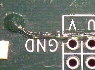
That was nifty work requiring a patient, steady hand. At the end of this row of plated-through holes, we milled down to layer 3 to expose the ground plane for the new bus connection. See Figure 3.
A tinned copper circuit was laid in the machined groove and carefully soldered to the underside of the pad for each plated-through hole. Once that was complete, the circuit was connected to ground.
That rework was visually inspected and electrically tested. Finally, the entire rework area was protected with high-strength thermoset epoxy.
So there it is, good stuff, done right and done quickly. One more fire quenched!