Introduction
This paper addresses the critical issue of component tinning, specifically focusing on its implementation and challenges. Authored by experts in the field, it provides valuable insights into the best practices and techniques required for successful lead tinning. As electronic components play a vital role across industries, ensuring reliable and efficient tinning is essential to maintaining their integrity and functionality.
The paper examines key factors, including temperature control, flux selection, and proper soldering techniques, providing practical guidelines and recommendations to address common tinning issues. By reviewing the intricacies of component lead thinning, this approach aims to equip professionals with the knowledge and strategies necessary to achieve optimal results in their tinning processes.
Details
The motivation behind component lead tinning is to facilitate the removal of gold plating, thereby eliminating the risk of gold embrittlement and mitigating tin whisker issues, and to process components for applications that require refinishing with lead-free solder for RoHS compliance. The component lead tinning process produces a homogeneous intermetallic layer on the base metal of component leads or terminations, thereby increasing overall solderability and improving the reliability of printed circuit board assemblies.
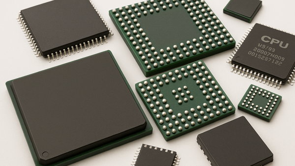
All leaded through-hole components, such as axial, radial, dual-inline package (DIP), or single-in-line package (SIP) devices, can be successfully re-tinned using the solder dip process. Surface-mount components that usually have terminations or pads but without leads, such as chip components, SOTs, SOICs, leaded chip carriers (LCC), or plastic leaded chip carriers (PLCC), can be re-tinned using the solder drag process. In many cases, fixturing is required to maintain parallelism during automatic re-tinning of surface-mount components.
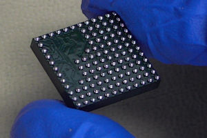
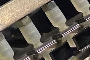
Multi-sided components, such as flat-pack (FP) and quad flat-pack (QFP) devices, have delicate leads that can be easily damaged. These components are re-tinned using a side-wave process, with components held in position by a multi-axis articulated robot equipped with a rotary vacuum head. Ball grid array (BGA) devices that require conversion from a lead-free finish to tin-lead to meet the requirements of defense or high-reliability applications must be re-balled. The first step in this conversion process is deballing, where the original solder balls are removed from the underside of the BGA devices, exposing the interposer pads.
A key issue when re-tinning fine-pitch surface-mount devices such as QFPs and quad flatpacks, no-lead (QFNs), is maintaining coplanarity across all leads while simultaneously ensuring bridge-free results. Fine-pitch QFPs as small as 6mm x 6mm with a lead pitch as small as 0.012” and up to 50mm x 50mm can be re-tinned with bridge-free results. Bottom-terminated devices such as QFNs as small as 3mm x 3mm with a lead pitch down to 0.5mm can be re-tinned with world-class coplanarity within 0.003” for these leadless devices. Device coplanarity and solder thickness from the re-tinning process should be verified using X-ray fluorescence (XRF) testing and alloy composition verification.
The critical process parameters for the component re-tinning process include:
- Control of the depth of immersion of the piece part in the flux bath
- Dwell time of the piece part is controlled in the preheat and the solder pot within ± 0.1 sec
- Control of entrance speed into the solder pot to within ± 0.3 cm/sec
- Depth of immersion of the piece part in the solder pot to within ± 0.1mm
- Optimum dwell time of the piece part in the solder pot to achieve an intermetallic bond
- Control of exit speed out of the solder pot to within ± 0.3 cm/sec
The temperature, flux chemistry, and extraction speed are crucial when removing through-hole or surface-mount components from the solder bath. These parameters play a significant role in controlling the thickness of solder applied by the re-tinning process.
It has been observed that some within the electronics assembly industry use a single static solder pot for both alloy removal and component re-tinning. This is not recommended since organic contaminants, flux buildup, and gold accumulation can be transferred to the re-tinned component leads or terminations. Those using this practice rely on outdated standards and procedures that do not comply with the GEIA-STD-0006 or IEC TS-62647-4 requirements for component re-tinning.
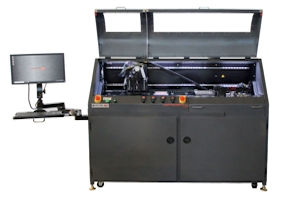
The ideal method for removing gold plating and mitigating tin whiskers from SMT and through-hole components is the robotic hot solder dip (RHSD) process. It is recommended that this retinning operation be carried out with a lead tinning machine, controlled flux application, preheating, single or dual solder pots, nitrogen insertion, and defined process control. A defined process of this type is highly recommended in place of manually dipping components into a standalone static solder pot to reduce solder contamination, minimize non-wetting issues, and enhance solderability.
Robotic hot-solder-dip (RHSD) machines can use either a single or a dual static or dynamic solder pot, with the first pot used to remove gold plating, oxidation, or other residues, and the second pot used for precise control of solder depth. An inert nitrogen atmosphere helps achieve a desirable solder finish while mitigating icicles and dross buildup. The immersion of the component lead or termination into the flux and solder should be controlled to allow the flux and solder to flow up the lead or termination to a predetermined depth. A defined withdrawal or extraction speed should be used in the second solder pot to control the re-tinning solder thickness. Solder pots should be tested regularly for copper, nickel, and other contaminants.
Robotic hot-solder dip tinning services can remove gold plating from through-hole and SMT component leads or pads, minimizing the risk of gold embrittlement as a failure mechanism. When using these robotic hot solder dip tinning services, it is recommended to use a batch wash system for post-process cleaning, as well as the following procedures:
- Component moisture sensitivity level (MSL) dry bake per J-STD-033
- Component moisture sensitivity level (MSL) packaging per J-STD-020
- Tape and reel packaging per EIA-481
If available from your robotic hot solder dip tinning service provider, the following testing services are beneficial and recommended to ensure process integrity:
- Ionic cleanliness (ROSE) testing per IPC-TM-650-2.3.25
- X-ray fluorescence (XRF) for alloy composition and finish thickness per JESD 213
- Solderability testing per J-STD-002
- Visual inspection
For ultra-high reliability, mission-critical applications such as military, security, defense, and/or aerospace, additional component testing services can be required utilizing the following test protocols:
- SAM (scanning acoustic microscopy) testing per J-STD-035
- Destructive physical analysis (DPA) per MIL-STD-1580
- Hermeticity testing (fine and gross leak) per MIL-STD-883
- Temperature, humidity, and bias testing
- Parametric testing
Conclusions
This paper addresses the critical issue of component tinning in the electronics industry. By highlighting the importance of proper lead tinning techniques, it underscores the significance of achieving reliable and robust solder joints. Through a comprehensive examination of key factors and best practices, it provides valuable insights into the successful implementation of component lead thinning.
This paper is a valuable resource for industry professionals seeking to enhance their tinning processes, emphasizing the importance of cleanliness, temperature control, and flux selection. Ultimately, implementing the recommended strategies and following the key success factors outlined in this paper can lead to improved solder joint quality and enhanced product reliability.
Several members of the Circuit Technology Center team contributed to this technical paper. Images may be altered or recreated to protect proprietary information.