Outline
This procedure is used to repair minor damage to circuit base board material. Scrapes and scratches in the base board material may be caused by accidents during handling. Burns in the base material may be caused by improper use of soldering and desoldering tools.
Caution: This method may be used when the damage extends deep into the base material but not completely through. If the baseboard material is damaged completely through, see Procedure No. 3.5.2 or 3.5.3.
Caution: Surface circuits may need to be replaced in the damaged area. Be sure that the appropriate circuit diagrams or photographs reflecting the original circuits are available so that they may be replaced after repairing the base board material. Damage to internal circuits or planes may have to be restored using surface wires.
Minimum Skill Level - Advanced
Recommended for technicians with soldering and component rework skills and exposure to most repair/rework procedures, but lacking extensive experience.Conformance Level - High
This procedure most closely duplicates the physical characteristics of the original, and most probably complies with all the functional, environmental and serviceability factors.| Procedure References | |
| 1-0 | 1.0 Foreword |
| 2-1 | 2.1 Handling Electronic Assemblies |
| 2-2 | 2.2 Cleaning Procedures |
| 2-5 | 2.5 Baking and Preheating |
| 2-7 | 2.7 Epoxy Mixing and Handling |
Tools and Materials

Ball mills, abrasives and cutting tools for working on circuit boards. |

Clear, superior strength epoxy in two-compartment plastic packages. |

General purpose cleaner for removing contamination. |

Disposable brushes for solvent cleaning and application of coatings. |

One part, semi-paste ink used to tint the color of epoxy and for direct printing on circuit board surfaces. |

Sturdy rack for PCBs used for rework and positioning. |

Swabs for use with solvents and application of color agents and epoxies. |

High temperature polyimide tape discs, .50" diameter. |

A must-have tool for precise cutting, scraping and trimming. |

Versatile power tool for milling, drilling, grinding, cutting and sanding. |

Precision microscope with stand and lighting for work and inspection. |

Disposable mixing sticks for mixing and applying adhesives. |

General purpose oven for drying, baking and curing epoxies. |

Nine precision-crafted tools for detailed circuit board work. |

Training kit to practice circuit board repair skills prior to testing for certification. |

Hardened stainless steel tip for scraping solder mask and removing defects. |

Nonabrasive, low-linting wipes for cleanup. |
Procedure
Procedure
- Clean the damaged area.
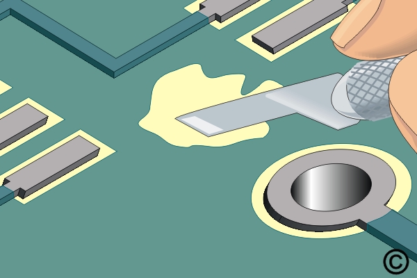
- Scrape away the damaged baseboard material using a knife. All damaged base board material and solder mask must be removed from the surface. (See Figure 1) or mill away the damaged base board material using the Micro-Drill System and ball mill. All damaged base board material and solder mask must be removed.
Note: To clearly see that all damaged material has been removed, flood the area with alcohol or solvent. Damaged internal fibers of the base material will show up clearly.
Caution: Abrasion operations can generate electrostatic charges.
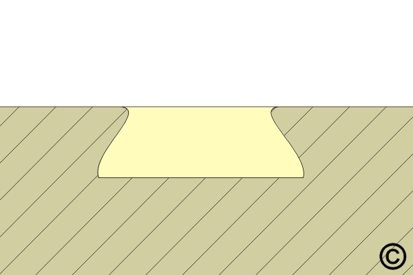
Note: An undercut to enhance mechanical strength may be desired for a class 3 product. (See figure 2) - Remove all loose material and clean the area.
- Where needed, apply High-Temperature tape to protect exposed parts of the circuit board.
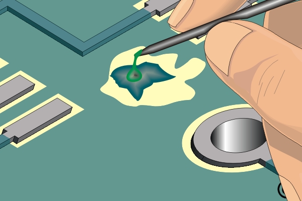
Note: The circuit Board may be preheated before filling the area with epoxy. A preheated PC board will allow the epoxy to easily flow and level out. Epoxy applied to an unheated circuit board may settle below the circuit board surface as the epoxy cures. - Mix the epoxy. If desired, add a color agent to the mixed epoxy to match the PC board color.
- Fill the area with epoxy up to and flush with the circuit board surface. No fibers of laminate material should be exposed. A mixing stick sharpened at the end may be used to apply and spread the epoxy. For large areas, apply the epoxy with a foam swab to create a textured surface. (See Figures 3 and 4)
Note: A slight overfill of epoxy may be desired to allow for shrinkage when the epoxy cures.
Note: Epoxy may be applied using a foam swab to restore the surface appearance. - Cure the epoxy per Procedure 2.7 Epoxy Mixing and Handling.
Caution: Some components may be sensitive to high temperatures. - After the epoxy has cured, remove the tape.
- If needed, use a knife or scraper and scrape off any excess epoxy. Scrape until the new epoxy surface is level with the surrounding circuit board surface.
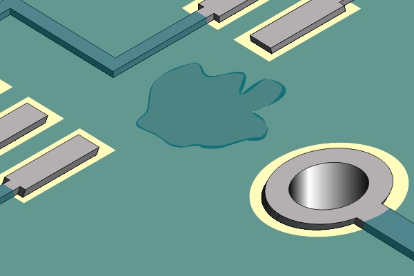
- Remove all loose material. Clean the area. (See Figure 5)
Note: If needed, apply an additional thin coating to seal any scraped areas.
Evaluation
- Visual examination for texture and color match.
- Electrical tests on conductors around the repaired area as applicable.
- No excess epoxy covering circuits or sensitive areas.
- Epoxy is fully bonded with no evidence of chipping.
Images