Outline
This method repairs mechanical or thermal blisters or delaminations in circuit board laminated base materials. The blister is sealed by injecting a low-viscosity epoxy into the blister/delamination void.
Caution: This method can only be used when the laminate base material has separated sufficiently, allowing the epoxy to flow throughout the void area.
Minimum Skill Level - Advanced
Recommended for technicians with soldering and component rework skills and exposure to most repair/rework procedures, but lacking extensive experience.Conformance Level - High
This procedure most closely duplicates the physical characteristics of the original, and most probably complies with all the functional, environmental and serviceability factors.| Procedure References | |
| 1-0 | 1.0 Foreword |
| 2-1 | 2.1 Handling Electronic Assemblies |
| 2-2 | 2.2 Cleaning Procedures |
| 2-5 | 2.5 Baking and Preheating |
| 2-7 | 2.7 Epoxy Mixing and Handling |
Tools and Materials

Ball mills, abrasives and cutting tools for working on circuit boards. |

Clear, superior strength epoxy in two-compartment plastic packages. |

Sturdy rack for PCBs used for rework and positioning. |

Precision microscope with stand and lighting for work and inspection. |

Disposable mixing sticks for mixing and applying adhesives. |

General purpose oven for drying, baking and curing epoxies. |

Polypropylene syringe barrels with stainless steel dispensing tips. |

Nonabrasive, low-linting wipes for cleanup. |
Procedure
- Clean the area.
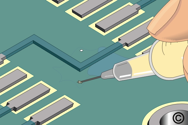
- Drill into the delamination blister with the Micro-Drill and ball mill. Drill in an area clear of circuitry or components. Drill at least two holes opposite each other around the perimeter of the delamination. (See Figure 1) Brush away all loose material.
Caution: Avoid drilling too deep, exposing internal circuits or planes.
Caution: Abrasion operations can generate electrostatic charges. - Bake the circuit board to remove any entrapped moisture. Do not allow it to cool before injecting the epoxy.
Caution: Some components may be sensitive to high temperatures. - Mix the epoxy. See the manufacturer's instructions on how to mix epoxy without bubbles.
Caution: Exercise care to prevent bubbles in the epoxy mixture. - Pour the epoxy into the epoxy cartridge.
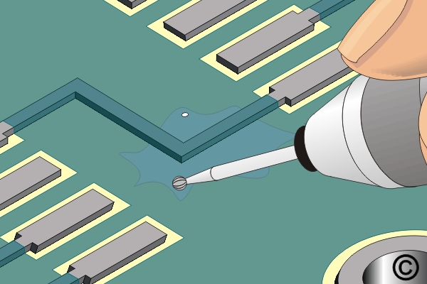
- Inject the epoxy into one of the holes in the delamination. (See Figure 2.) The heat retained in the circuit board will improve the flow characteristics of the epoxy and draw it into the void area, filling it completely.
- If the void does not fill, the following procedures may be used:
- Apply light local pressure on the board surface starting at the fill hole, slowly proceeding to the vent hole.
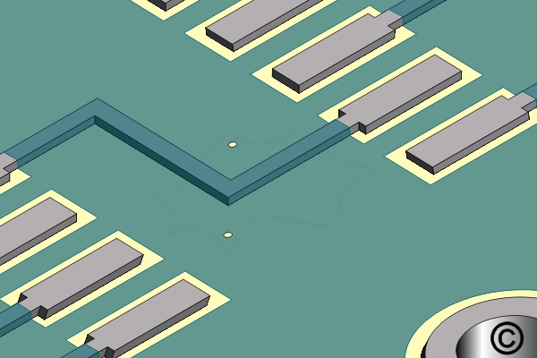
- Apply a vacuum to the vent hole to draw the epoxy through the void. - Cure the epoxy according to Procedure 2.7 Epoxy Mixing and Handling. Using a knife or scraper, scrape away any excess epoxy.
Note: If needed, apply an additional thin coating to seal any scraped areas.
Evaluation
- Visual examination for texture and color match.
- Electrical tests to conductors around the repaired area as applicable.
Images

Delamination/Blister Repair, Injection Method
Drill into the delamination blister with the Micro-Drill and ball mill.
Inject the epoxy into one of the holes in the delamination.
Cure the epoxy per the manufacturer's recommendation.