Abstract
The economic and environmental implications of electronic component salvage and reuse are becoming increasingly significant amid rising semiconductor and artificial intelligence chip costs and sustainability concerns. This paper examines the feasibility and benefits of salvaging and reconditioning the leads and pads of electronic components, with a focus on high-value components such as microprocessors, microcontrollers, and artificial intelligence chips. The paper outlines key steps, including the selective removal of soldered components, reconditioning of component leads, pins, and pads, marking harvested components to facilitate tracking and traceability, and repackaging for use with automated circuit board assembly equipment.
This study will evaluate the costs involved to allow for a comparison with the use of newly fabricated components, highlighting potential savings in materials and energy. Using salvaged components significantly reduces the costs associated with producing new microprocessors.. In addition to economic advantages, salvaging offers considerable environmental benefits. It mitigates the energy-intensive processes associated with new chip fabrication and reduces the need for costly ultra-purified water, a critical resource in semiconductor manufacturing. By extending the lifecycle of electronic components, salvage and reuse contribute to a more sustainable electronics industry and align with broader environmental goals. This paper provides a comprehensive analysis of the processes, costs, and benefits, underscoring the viability of electronic component reclamation as both a cost-saving and environmentally responsible practice.
Standards Development
The proposal for developing a component reclaim standard was initially brought to the V-ESSC European Standards Steering Committee for open discussion. A standardized set of requirements and guidelines was proposed to ensure the reliability of reclaimed components and to provide customers with confidence when purchasing and using them. The V-ESSC group discussed the topic, and many members agreed to bring it to the IPC 7-34 Repairability Subcommittee for further exploration. The IPC committee suggested having this information and requirements in a separate document, which led the IPC to seek input from worldwide industry-leading electronic reclamation facilities and experts [1]
Electronics Waste and Circularity
The IPC effort to create this standard started with an urging from IPC staff. There have also been discussions related to this effort at IEEE, INEMI, and with governments and municipalities worldwide. These groups are working on circularity, which is described as the ability to reuse rather than recycle electronic waste. If high-value electronic components can be harvested from scrap circuit boards and reused, it extends their lifespan. Reuse reduces the high energy usage required to fabricate new electronic components. A pressing challenge in electronics circularity is the rapid pace of technological change. This is an issue for the electronics manufacturing industry since circular pathways close rapidly, affecting all aspects of the industry, including manufacturers and consumers. Repairability, the use of secondary materials, reuse, and resource efficiency during manufacturing enable the reuse of materials in the next generation of products, thereby avoiding landfilling [2].
Linear design thinking has no environmental impact when electronic components are used for a single manufacturing lifecycle. Design for disassembly (DfD) is a time shift in which linear design thinking is replaced by circular design thinking, which leads to recycling without crushing and burning electronic components to extract raw materials. Rather, circular design thinking and DfD look for repairable, upgradeable, or reusable components. In effect, DfD seeks methods for extending the usable life of products, components, and materials [3]
Component Removal
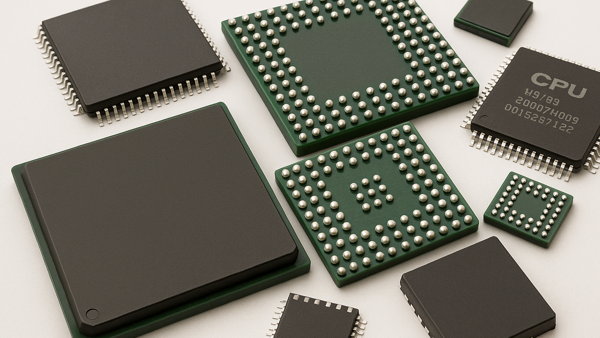
Beyond simple mechanical disassembly, nearly all electronic components harvested for reuse will be soldered directly to circuit board substrates. There are many methods for safely and efficiently removing soldered electronic components using convection and conduction. See Figures 1 and 2. To meet the requirements of purchasers and reusers of electronic components, the processes used to remove components must fall within the limits established by the original component manufacturer. In addition, purchasers will require that the processes used to harvest the components are environmentally responsible, processed using proper electrostatic controls, and documented. Where possible, the components will be marked to provide a level of tracking and traceability.
Component Lead and Pad Re-Conditioning
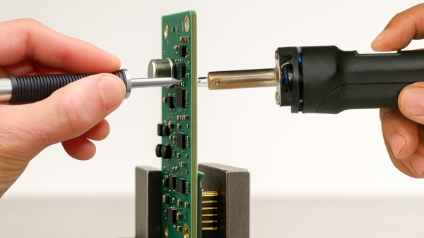
After soldered components are removed, the leads, pins, or pads of the components will not usually meet the components' original stated specifications. There may be excessive or insufficient solder, so the leads, pins, or pads will require reconditioning. Robotic hot-solder dip processing is appropriate for various component lead reconditioning processes, including restoring the lead, pin, or pad solder plating alloy and thickness specifications. See Figures 3 and 4. Robotic hot-solder dip processing is also an effective method for removing and preparing pads on ball grid array (BGA) components, thereby preparing them for solder ball replacement. Automated robotic hot-solder-dip component lead tinning systems are typically MIL-spec-compliant, meeting MIL-PRF-38535, MIL-PRF-38524E, and EIA/IPC/JEDEC J-STD-002E standards.[4]
Automated lead conditioning and BGA pad preparation can be performed simultaneously on multiple components using a robotic hot-solder-dip system equipped with multi-component vacuum pickup heads and dynamic solder waves. Process parameters can be accurately controlled including immersion depth, dwell time, insertion and extraction speeds, acceleration, solder pump speed, and temperature, ensuring the process complies with stringent industry standards including GEIA-STD-0006, J-STD-001, and IEC TS 62647-4:2018 Process management for avionics - Aerospace and defense electronic systems containing lead-free solder - Part 4: Ball grid array (BGA) re-balling [5].
Various methods, including fixtures and laser systems, are available for re-attaching solder spheres after the pads of ball grid array components have been prepared. Solder ball count, device pitch, solder sphere diameter, solder alloy, and package size are all considerations when selecting the appropriate method for a particular application. See Figure 5.
Following deballing and reballing, various inspection steps are performed, including Z-height measurement of solder balls. Other common high-value surface-mount components, including J-lead, gull-wing, and various flat-pack formats, often have delicate leads that can be easily damaged. These devices may require lead repositioning and retinning using a side-wave process, with components held in position by a multi-axis articulated robot equipped with a rotary vacuum head.
Following robotic hot solder dip processing, all reconditioned components are cleaned in batch or inline cleaning systems using the appropriate solvent or aqueous cleaning agent to remove residual flux residues. Baking may be required to meet component moisture sensitivity levels. Additional testing may be conducted, including solderability testing as specified in J-STD-002. Further processing of reconditioned components may involve component MSL (Moisture Sensitive Level) testing, dry baking per J-STD-003D, tape-and-reel packaging per ANSI/EIA-481E, and packaging in vacuum-sealed barrier bags with desiccant and moisture indicator cards per J-STD-020F.
Economic Value Proposition
The economic and environmental benefits of using harvested electronic components instead of original equipment manufacturer (OEM) components can be substantial and encompass several key factors. In addition to reducing e-waste, salvaging and reconditioning high-value components provide significant energy savings. According to industry estimates, it takes approximately 1,500 to 2,500 kWh of energy to produce a single 300 mm-diameter semiconductor wafer. Assuming a wafer produces 500 chips on average, the energy used per chip would be roughly 5 kWh. However, this figure can vary depending on the manufacturing process and the chip's size and complexity.
This estimate only accounts for fabrication and does not consider other factors, such as the energy required for raw material extraction, transportation, or packaging. The actual energy usage might be higher when these additional stages are considered. There are several steps in the component harvesting process, including mechanical disassembly, selective removal of the soldered components, reconditioning of component leads and pads, marking of the parts that have been salvaged to provide tracking and traceability, testing, and finally, the repackaging in tubes, trays or other packaging for use with automated circuit board assembly equipment.
For this examination, the labor times and cost calculations are based on reclaiming electronic components from circuit board assemblies removed from their enclosures. Labor times can vary considerably depending on the complexity of the dismantling process to expose the individual circuit board, so those added costs are not included. Additionally, these calculations are based on reclaiming five components of each component type from 200 circuit board assemblies, for a total of 1000 components of each type. Smaller quantities would increase labor time, and larger quantities would decrease labor time, which would impact overall costs. These labor time calculations use modern production-based equipment and fully trained, experienced technicians and operators.
Component Reclaim Equipment and Processes
Various tools and machines are required to reliably reclaim soldered electronic components from circuit boards. These include cleaning systems, baking ovens, microscopes, inspection systems, handling equipment, and various small tools. Table 1 lists the tools and primary machines needed to efficiently and reliably reclaim various component types. Table 2 lists approximate labor times and costs for component reclaim.
Table 1. Component Reclaim Equipment and Processes
| Chip Components |
Manual conduction/hot air solder rework tools; robotic hot solder dip systems. |
| Through-Hole Components |
Mini solder wave systems; robotic hot solder dip systems. |
| SMT Components, up to 10 leads |
Manual/semi-automatic hot air rework systems; robotic hot solder dip systems. |
| SMT Components, greater than 10 leads |
Manual/semi-automatic hot air rework systems; robotic hot solder dip systems. |
| BGA Components, up to 100 balls |
Manual/semi-automatic hot air rework systems; robotic hot solder dip systems; BGA reball fixtures; inline/batch reflow ovens. |
| BGA Components, greater than 100 balls |
Manual/semi-automatic hot air rework systems; robotic hot solder dip systems; BGA reball fixtures; inline/batch reflow ovens. |
Table 2. Approximate Component Reclaim Labor Time and Costs
| Chip Components |
8 minutes/component |
$14.00/component |
| Through-Hole Components |
34 minutes/component |
$59.50/component |
| SMT Components, up to 10 leads |
19 minutes/component |
$33.25/component |
| SMT Components, greater than 10 leads |
25 minutes/component |
$43.75/component |
| BGA Components, up to 100 balls |
27 minutes/component |
$47.25/component |
| BGA Components, greater than 100 balls |
35 minutes/component |
$61.25/component |
Table 2 sets the fully burdened labor rate for this examination at $80.00 per hour. The equipment amortization rate is estimated at $25.00 per hour, bringing the total hourly average cost to $105.00. Labor time and average cost are estimated and may vary considerably.
Sustainability
Electronic waste is a global problem, and consumers are driven to acquire the latest technology. In response, the electronics manufacturing industry is shifting towards greener practices, as noted in June 2024, when researchers, policymakers, and industry leaders met at the EGG "Electronics Goes Green 2024+" conference in Berlin, Germany. The conference focused on sustainability for the electronics, information, and communications technology industries. As technology rapidly evolves, it is vital that the electronics manufacturing sector prioritizes environmental considerations and promotes eco-friendly practices throughout its value chain. This includes adopting circularity and encouraging the longevity of electronic products, as well as adopting design principles for longevity and energy efficiency. This approach reduces the product's carbon footprint by promoting the reconditioning and reuse of reclaimed electronic components.[7]
Industry Acceptance
The key to acceptance of reclaimed electronic components for reuse within printed circuit assembly operations will primarily be driven by trust. The purchasers of reclaimed components must trust that the components were harvested following high-quality controls and within specified limits. Critical factors that will improve the acceptance of harvested components within the electronics assembly community include, where possible, markings to distinguish harvested components from OEM devices, the assembly facilities' ability to identify the source of the harvested components, the qualifications and certifications of the component reclamation facility, and assurances that the harvested components are not counterfeit.
Conclusion
This paper has provided a comprehensive and insightful analysis of the economic and environmental implications of electronic component salvage and reuse. While the economics of reclaiming many low-cost components may not offer a positive return, there is a clear value proposition in reclaiming electronic components with higher values, including microprocessors, microcontrollers, and artificial intelligence semiconductor chips. The authors focus on the processes, costs, and benefits of reusing reclaimed electronic components, offering valuable insights into the future direction of the electronics manufacturing industry in advancing a sustainable electronics future. Adhering to high-quality standards throughout the reclamation process is crucial to maintaining the integrity of the electronic component supply chain. It will reduce reliance on energy-intensive processes for newly fabricated components.
Acknowledgements
The authors would like to acknowledge Francisco Fourcade of IPC and the staff members of Circuit Technology Center, Inc., for their contributions to this paper.
References
[1] IPC-7712 Component Reclaim Standard, under development, Fourcade, Francisco, Staff Liaison and Group Manager, IPC International, Inc.
[2] Scanlon, Kelly, and Schaffer, Mark, "Circularity Challenges in Electronics Manufacturing," IPC and iNEMI, Berlin, Germany, July 17, 2024 https://www.ipc.org/event/circularity-challenges-electronics-manufacturing
[3] Cadence PCB Design & Analysis Blog, "Design for Disassembly, Circular Design, and Product Lifecycle Management"; Cadence PCB Solutions, April 16, 2020 https://resources.pcb.cadence.com/blog/2020-design-for-disassembly-circular-design-and-product-lifecycle-management
[4] Henry, Reid, "The Critical Role of Robotic Hot Solder Dip Processing for Components for High-Reliability and Mission-Critical Applications," Hentec Industries/RPS Automation, September 2023 https://rpsautomation.com/wp-content/uploads/2023/09/The-Critical-Role-of-RHSD-in-High-Reliability-Applications.pdf
[5] Price, Andy, LePage, Bob, Cormier, David, and Rennick, Jim, "The Essential Guide for High-Reliability BGA Component Re-Balling," Circuit Technology Center, Inc., March 2022 https://www.circuitrework.com/tech-papers/1040.html
[6] Figures 1, 2, 3, 4, and 5: Source: Circuit Technology Center, Inc.
[7] Global IMI Blog, "How Green Can Electronics Get in 2024?" Integrated Micro-Electronics, Inc., April 23, 2024 https://www.global-imi.com/blog/how-green-can-electronics-get-2024
Several members of the Circuit Technology Center team contributed to this technical paper. Images may be altered or recreated to protect proprietary information.