Circuit Technology Center
SEARCH  

4.2.3 Conductor Repair, Welding Method

 
Outline
This procedure is used to repair short breaks or opens in circuits on circuit boards. A parallel gap welder is used to weld a jumper ribbon across the damaged conductor.

Caution: Welding current and voltages may affect component reliability on assembled circuit boards. The repaired section must not reduce the circuit width, spacings, or current carrying capacity below the allowable tolerances.

Caution: Subminiature parallel gap welding is extremely sensitive to the proper placement of the electrode tip. Inconsistent welds can occur due to poor electrode tip placement, incorrect tip size, or improper weld settings.

Preparation: Prior to using any welding equipment, certain precautions should be taken. The equipment should have electrodes cleaned, aligned, and set for the proper board thickness.

Test samples that have similar circuit widths, spacing, thickness, surface finish, contour, etc. Observe and test the weld quality, alignment, discoloration, fusion, and the appearance of the base material in the area of the weld. Readjust the weld equipment settings and repeat until acceptable results have been achieved.

The alignment of the welded ribbon to the circuit pattern should be within 0.050 mm (.002"). The weld bond strength should exceed the circuit/base material bond strength.

Minimum Skill Level - Advanced
Recommended for technicians with soldering and component rework skills and exposure to most repair/rework procedures, but lacking extensive experience.

Conformance Level - High
This procedure most closely duplicates the physical characteristics of the original, and most probably complies with all the functional, environmental and serviceability factors.

Acceptability References
IPC-A-600 2.0 Externally Observable Characteristics
IPC-A-610 10.0 Laminate Conditions
Procedure References
1.0 Foreword
2.1 Handling Electronic Assemblies
2.2 Cleaning
2.7 Epoxy Mixing and Handling
IPC7721 4.2.3 Conductor Repair, Welding Method
Kits and Systems
110-6380
Flex-Rack PCB Holder
Sturdy holder supports PCBs for rework, drilling, pad repair, and positioning.
201-7100
Precision Tool Set
Nine precision-crafted tools for detailed circuit board work.
Tools and Materials
115-3136
Abrader
Mild abrasive for removing oxides and contaminants.
235-2106-5
Cleaning Brushes
Disposable brushes for solvent cleaning and application of coatings.
115-3302
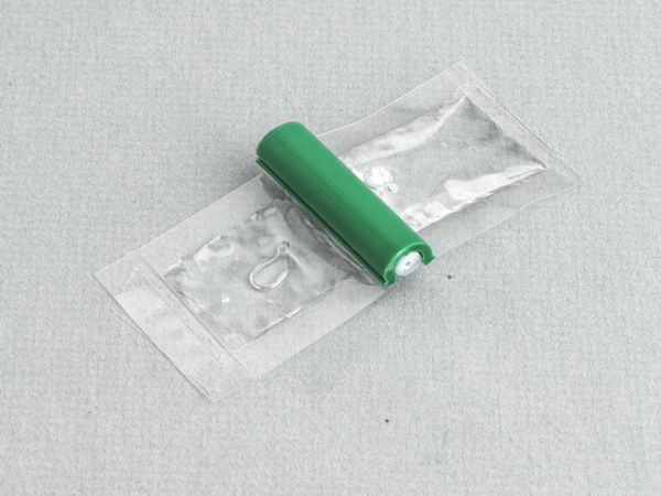
Circuit Bond Epoxy
Clear, superior strength epoxy in two-compartment plastic packages.
355-0614
Knife with #16 Blades
A must-have tool for precise cutting, scraping and trimming.
Additional Items and Supplies
Cleaner
Cleaner
General purpose cleaner for removing contamination.
Solderinmg Iron
Soldering Iron
Properly maintained soldering iron and properly sized soldering iron tips.
Hot Plate
Tweezers
Multiple sizes and tip configurations of tweezers for various small parts handling needs.
Wipes
Wipes
Nonabrasive, low-linting wipes for cleanup.
Circuit Bond Epoxy
Circuit Bond is a clear, low viscosity, superior strength epoxy precisely measured out into two-compartment plastic packages, so it's easy to use, and there's no measuring. For over a decade, this high-strength epoxy has been qualified and used by thousands of high-rel electronics manufacturers across the globe.
1. Circuit Bond has a working pot life of 30 minutes. It should not be mixed until ready to use.
2. To use Circuit Bond, remove the plastic clip separating the resin and hardener. Squeeze back and forth from one half of the package to the other to mix the contents.
3. Cut a corner off the package and squeeze all the contents into a Plastic Cup. Stir the contents to ensure it is thoroughly mixed.
4. Circuit Bond may contain bubbles from the mixing process. If needed, use a vacuum system to remove bubbles.
5. Color Agent can be mixed in with Circuit Bond to match surface colors if desired.
6. Apply using a Foam Swab, Micro Probe, or Mixing Stick as required.
7. Cure Circuit Bond for 24 hours at room temperature or 4 hours at 65°C (150°F).
Specifications
Packaging2 gram pre-measured packages
Mix ratio4 parts resin to 1 part hardener
Mix Ratio by Weight (R/H)100/25
ColorClear, transparent
Pot life30 minutes
Cure cycle24 hours at room temp (25 °C) or 4 hours @ 65°C
Thixotropic Index1
Specific Gravity1.20
Percent Solids100%
Viscosity (after mixing)2000 cps
Operating temperature range-55°C to 135°C
Hardness88 Shore D
Lap Shear, Alum to Alum1100 psi
Glass Transition Temperature, Ultimate92°C
Coefficient of Expansion, cm/cm/°C6 E-05
Dielectric strength400 volts/mil
Dielectric Constant, 1KHz@25°C4
Shelf Life6 months minimum
Procedure
  1. Clean the area.
  2. Select a section of Kovar ribbon of the same width as the conductor pattern being repaired +/- .050 mm - 0.002".
  3. Cut the ribbon approximately 3.0 mm (.120") longer than the section being repaired.
  4. Clean the ribbon conductor and base material surrounding the repair area.
  5. Place and center the ribbon over the section to be repaired, leaving equal ribbon end lengths on each side and parallel to the circuit pattern.
  6. Place the circuit board under the weld electrodes so that the electrodes are depressed to the area of the weld.
  7. Hold the ribbon in place with the Precision Tweezers until the weld is completed. Weld in place using settings based on the accepted test samples.
  8. Clean the area.
  9. Carefully inspect the joint for weld quality and alignment.
  10. If required, apply a small amount of flux and tin the entire area with solder.
  11. Clean the area.
  12. Coat the repaired area with epoxy if needed.
Evaluation
  1. Visual examination, dimensional measurement of conductor width and spacing, and electrical continuity measurement.
Procedure for reference only.