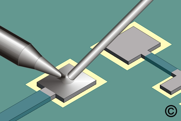
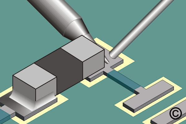
7.3.1 Soldering Surface Mount Chip Components, Point To Point Method
Install surface mount chip components using controlled point-to-point soldering techniques. Covers pad preparation, alignment and heat management for reliable attachment.
Minimum Skill Level: Intermediate
Conformance Level: High
REQUEST FOR QUOTE GUIDES INDEX