Circuit Technology Center 22 Parkridge Road
Haverhill, MA 01835 USA
www.circuitrework.com

4.7.2 Surface Mount Pad Repair, Film Adhesive Method

Procedure covers method to repair damaged surface mount pads on circuit board assemblies using dry film adhesive.

Minimum Skill Level: Advanced
Conformance Level: High


REQUEST FOR QUOTE    GUIDES INDEX
slide 1
Surface Mount Pad Repair, Film Adhesive Method
slide 2
Remove the defective pad and remove soldermask from the connecting circuit.
slide 3
Select a replacement pad that matches the missing pad.
slide 4
Scrape off the adhesive bonding film from the solder joint area on the back of new pad.
slide 5
Cut out the new surface mount pad. Cut from the plated side.
slide 6
Place the new surface mount pad in place using Kapton tape.
slide 7
Completed repair.
generic
Circuit Frames have a dry-film adhesive backing to ensure the delicate repair procedure is easy, fast, and highly reliable LEARN MORE
micro-drill
You'll appreciate the accuracy of this precision machine when repairing conductors, lands, and surface mount pads. LEARN MORE
generic
We're here to help with all your challenging circuit board and electronic component rework and repair needs. LEARN MORE
SLIDESHOW STARTING
Outline

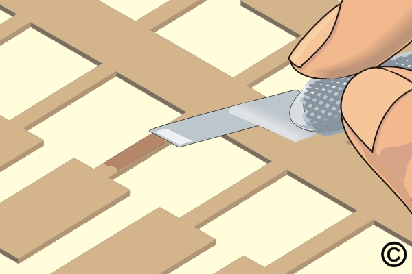
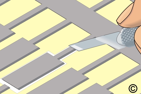
This method replaces damaged surface mount pads with new adhesive-backed dry film pads. The new pads are bonded to the circuit board surface using a bonding iron.

Caution: It is essential that the board surface be smooth and flat. If the base material is damaged, see the appropriate procedure.

Note: This method uses replacement surface mount pads. The new pads are fabricated from copper foil. They are available in many sizes and shapes and are generally supplied solder plated.

Minimum Skill Level - Advanced
Recommended for technicians with soldering and component rework skills and exposure to most repair/rework procedures, but lacking extensive experience.

Conformance Level - High
This procedure most closely duplicates the physical characteristics of the original, and most probably complies with all the functional, environmental and serviceability factors.

Acceptability References
IPC-A-600 2.0 Externally Observable Characteristics
IPC-A-610 10.0 Laminate Conditions
Procedure References
1.0 Foreword
2.1 Handling Electronic Assemblies
2.2 Cleaning
2.5 Baking And Preheating
2.7 Epoxy Mixing and Handling
IPC7721 4.7.2 Surface Mount Pad Repair, Film Adhesive Method
Tools, Materials and Supplies

Procedure
  1. Clean the area.
  2. Remove the defective pad and a short length of the connecting circuit. (See Figure 1)
  3. Use a knife and scrape off any epoxy residue, contamination, or burned material from the board surface.
  4. Scrap any solder mask or coating from the connecting circuit. (See Figure 1)
  5. Clean the area.
  6. Apply a small amount of liquid flux to the connection area on the board surface and tin with solder. Clean the area. The length of the overlap solder connection should be a minimum of 2 times the circuit width.
  7. The area for the new pad on the board surface must be smooth and flat. If internal fibers of the board are exposed, or if there are deep scratches on the surface, they should be repaired. Refer to the appropriate procedure.
  8. Select a replacement surface mount pad that most closely matches the original surface mount pad. If a special size or shape is needed, they can be custom fabricated. (See Figure 2) 
    Note: New surface-mount pads are fabricated from copper foil. The foil is plated on the top with solder, and an adhesive bonding film is applied to the bottom.
  9. Before trimming out the new pad, carefully scrape off the adhesive bonding film from the solder joint connection area on the back of the new pad. (See Figure 3)
    Caution: Scrape off the epoxy backing only from the joint connection area. Avoid touching the epoxy backing with your fingers or other materials that may contaminate the surface and reduce the bond strength when handling the replacement contact.
  10. Cut out and trim the new pad. Cut out from the plated side. Cut the length to provide the maximum allowable circuit overlap for soldering. Minimum two times the circuit width. (See Figure 4)
  11. Place a piece of High-Temperature Tape over the top surface of the new pad. Place the new pad into position on the circuit board surface using the tape to help in alignment. (See Figure 5)
  12. Select a bonding tip with a shape to match the shape of the new pad. See the bonding tip chart in the replacement parts section of the manual provided with the repair system or repair kit.
    Note: The tip used for bonding should be as small as possible, but should completely cover the entire surface of the new pad.
  13. Position the circuit board so that it is flat and stable. Gently place the hot bonding tip onto the High-Temperature Tape covering the new pad. Apply pressure as recommended in the manual of the repair system or repair kit for 5 seconds to tack the new pad in place. Carefully peel off the tape. 
    Caution: Excessive bonding pressure may cause measling in the circuit board surface or may cause the new pad to slide out of position.
  14. Gently place the bonding tip directly onto the new pad. Apply pressure as recommended in the manual of the repair system or repair kit for an additional 30 seconds to bond the pad fully. After the bonding cycle, the new pad is fully cured. Carefully clean the area and inspect the new pad for proper alignment.
  15. If the new pad has a connecting circuit apply a small amount of liquid flux to the lap solder joint connection area and solder the circuit from the new pad to the circuit on the circuit board surface. Use minimal flux and solder to ensure a reliable connection. Tape may be placed over the top of the new pad to prevent excess solder overflow.
    Note: If the configuration permits, the overlap solder joint connection should be a minimum of 3.00 mm (0.125") from the related termination. This gap will minimize the possibility of simultaneous reflow during soldering operations. Refer to 7.1 Soldering Basics.
  16. Mix epoxy and coat the lap solder joint connection. Cure the epoxy per Procedure 2.7 Epoxy Mixing and Handling.
    Note: Additional epoxy can be applied around the perimeter of the new pad to provide additional bond strength.
    Caution: Some components may be sensitive to high temperatures.
  17. Apply surface coating to match prior coating as required.

Evaluation

  1. Visual examination.
  2. Measurement of new pad width and spacing.
  3. Electrical continuity measurement.
Images and Figures
Surface Mount Pad Repair, Film Adhesive Method
Remove the defective pad and remove soldermask from the connecting circuit.
Figure 1. Remove the defective pad and remove soldermask from the connecting circuit.
Select a replacement pad that matches the missing pad.
Figure 2. Select a replacement pad that matches the missing pad.
Scrape off the adhesive bonding film from the solder joint area on the back of new pad.
Figure 3. Scrape off the adhesive bonding film from the solder joint area on the back of new pad.
Cut out the new surface mount pad. Cut from the plated side.
Figure 4. Cut out the new surface mount pad. Cut from the plated side.
Place the new surface mount pad in place using Kapton tape.
Figure 5. Place the new surface mount pad in place using Kapton tape.
Completed repair.
Figure 6. Completed repair.
Contact Us/Quote Request


Send Documents *
No file chosen
No file chosen
No file chosen
No file chosen
No file chosen

Notes/Questions/Requests

Product Type
Assemblies Bare PCBs Other

Quantity

Delivery Schedule Request
3 Weeks 2 Weeks 1 Week
2-3 Days 1 Day

Security Check


* You may upload PDFs and other file types (max 4 MB each). For multiple files, zip them or send to info@circuitrework.com

Form Security
Our forms run on AWS with an industry-leading firewall. Data is encrypted at rest with AES-256 and in transit using TLS 1.2+.