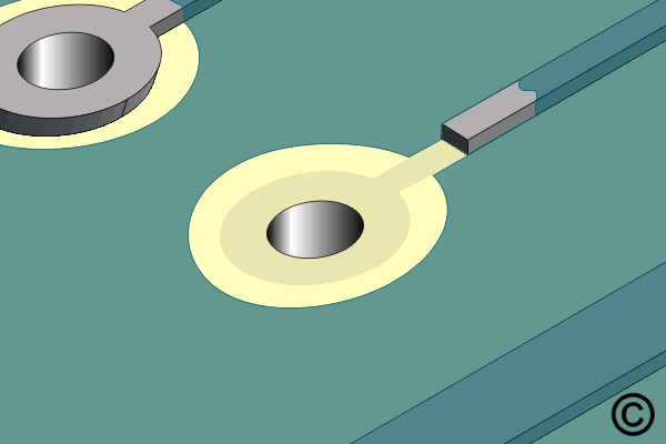
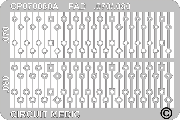
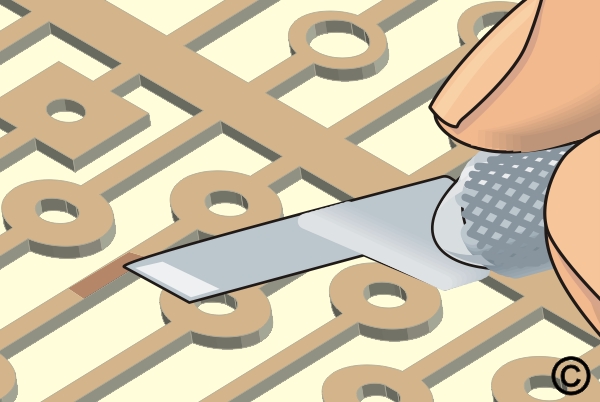
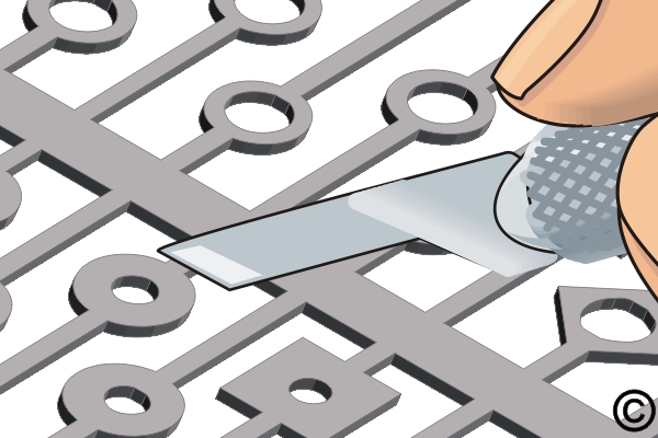
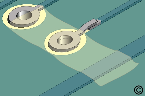
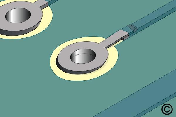
4.5.2 Land Repair, Film Adhesive Method
Restore edge contacts using replacement patterns bonded with film adhesive. Learn alignment and finishing practices to maintain reliable edge connector performance.
Minimum Skill Level: Advanced
Conformance Level: High
REQUEST FOR QUOTE GUIDES INDEX