This method is used for replating edge contacts by selective swab plating. Edge contacts may require replating if they become contaminated with solder or are scratched during handling. Other applications may arise when the plating on the edge contacts does not meet the minimum thickness specification or if the specification changes.
This electroplating process uses a DC power supply. One lead is connected to the connector edge contacts that need plating. A second lead is connected to the plating probe. The plating probe has an anode fastened to the tip. The anode has absorbent wrapping. The anode is dipped into high-speed proprietary plating solutions. When the saturated anode is swabbed across the circuit board connector edge contacts, the metal contained in the solution is plated wherever electrical contact is made. Before relating, any solder contamination must be removed.
Caution: This method can be used to replate any metal surface, including connector edge contacts, but it is essential that the surface to be plated is free of deep scratches, nicks, pin holes or other defects. If the edge contacts need to be replaced, see the appropriate procedure.
Minimum Skill Level - Advanced
Recommended for technicians with soldering and component rework skills and exposure to most repair/rework procedures, but lacking extensive experience.
Conformance Level - High
This procedure most closely duplicates the physical characteristics of the original, and most probably complies with all the functional, environmental and serviceability factors.
|
| Acceptability References |
| IPC-A-600 2.0 |
Externally Observable Characteristics |
| IPC-A-610 10.0 |
Laminate Conditions |
|
|
|
| Tools, Materials and Supplies |
|
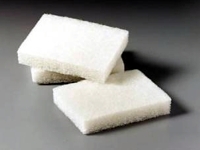
Abrasive Pads
Light duty abrasive scrubbing pads to remove contamination and blend surfaces.
|
Buss Wire, 30 AWG
Used to create buss connection during plating.
|
Flex-Rack PCB Holder
Sturdy rack for PCBs used for rework and positioning.
|
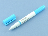
Conductive Pen
Pen dispenser for creating conductive silver traces.
|
Cleaner
General purpose cleaner for removing contamination.
|
Desolder Braid
Woven copper wire designed to wick solder from surfaces and holes.
|
Gloves
Disposable, puncture-resistant gloves designed for handling mild chemicals.
|
Gold Contact Plating Kit
Kit to repair damaged gold contacts and pads on circuit boards.
|
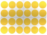
High Temp Tape Discs
High temperature polyimide tape discs, .50" diameter.
|
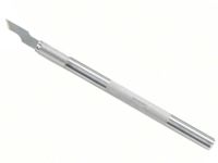
Knife with #16 Blades
A must-have tool for precise cutting, scraping and trimming.
|
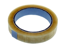
Tape, Peel Test
This tape is specifically designed to test plating adhesion.
|
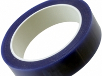
Tape, Plating and Masking
Ideal for masking during plating, coating removal and microblasting.
|
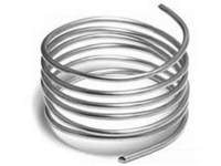
Plating Solutions and Anodes
Plating tools, plating anodes and various plating solutions for gold contact repair.
|
Precision Tool Set
Nine precision-crafted tools for detailed circuit board work.
|
Safety Glasses
Protect your eyes and your vision with proper safety glasses.
|
Soldering Iron
Properly maintained soldering iron and properly sized soldering iron tips.
|
Wipes
Nonabrasive, low-linting wipes for cleanup.
|
|
Procedure
Safety
- This procedure should be thoroughly reviewed before attempting repairs. Technicians should become familiar with the tools and should practice on scrap circuit boards.
- A clean work environment is essential for the best results. A smooth work surface and good lighting are recommended.
- Safety glasses and safety gloves should always be worn when handling hazardous chemicals.
- The work area should be adequately ventilated. If ventilation is inadequate, use a fan to move fumes away from the operator.
Setup
- To prevent contamination of probe ends, it is important to label the Plating Probes based on the solution used.
- Properly rinse Plating Probes after each use to prolong anode life.
- Do not rinse hazardous chemicals down the drain. Follow local and federal regulations regarding waste disposal.
Preparation - Remove Solder Contamination
Caution: Safety glasses and safety gloves should always be worn when handling hazardous chemicals. Do not work within a small enclosed room without supplemental ventilation. If ventilation is inadequate, use a fan to move fumes away from the operator.
- Clean the rework area.
- Apply plating tape to the circuit board surface surrounding the area to be reworked. The plating tape will protect adjacent components and the circuit board surface from unwanted exposure to stripping and plating solutions.
- Using a soldering iron, flow solder over any contaminated contact area. This provides a more even surface when plating. Remove the bulk of the solder contamination using desoldering tools or desoldering braid. (See Figure 2)
- Clean the area.
- Place the circuit board so that the leading edge overhangs a tray to collect runoff solution.
- Swab the solder stripping solution over the solder contamination using a swab. Swab the surface until all remaining solder has been stripped off. (See Figure 3)
- Thoroughly rinse the entire area with water. (See Figure 4)
- Mildly buff the contacts using an abrasive pad. Mild buffing will prepare the surface for plating and remove any remaining solder contamination.
- Thoroughly rinse with water to remove any residue.
Preparation - Remove Poor Plating or Surface Defects
- Clean the rework area.
- Apply plating tape to the circuit board surface surrounding the area to be reworked. The plating tape will protect adjacent components and the circuit board surface from unwanted exposure to stripping and plating solutions.
- Clean the area.
- Buff the contacts using an abrasive pad. Buff the contacts until all defective or poor plating is removed.
- Burnish small scratches. Use the tip of the Burnisher to work the copper material into the scratch and smooth out the area. Finish by mildly buffing the area to remove any minor burnishing marks. If there are large scratches, the contact may need replacement. See Procedure Number 4.6.1 or 4.6.2.
- Thoroughly rinse the entire area with water to remove any residue.
Electrical Buss Connection
A conductive bus must be made to all the contacts that need plating. Making a reliable bus connection is the most important step in plating. All sorts of problems will be eliminated by taking the time to make a reliable bus connection. There are four basic connectivity options.
Busing - Wire Soldered to Edge (Option 1)
Caution: When finished, this method will leave a small unplated line along the inner tip of each contact.
- Apply high-temperature tape to all the contacts to be plated. The high-temperature tape should cover the entire contact except for a small line along the inboard edge. The high-temperature Tape will prevent further solder contamination.
- Solder a 30 gauge wire directly to the inboard tip or connecting circuit of each contact to be plated. The smallest amount of solder should be used to prevent further contamination. (See Figure 5)
Busing - Conductive In Applied to Edge (Option 2)
Caution: When finished, this method will leave a small unplated line along the inner tip of each contact.
- Apply High-Temperature Tape tape to all the contacts to be plated. The High-Temperature Tape should cover the entire contact except for a small line along the inboard edge. The High-Temperature Tape will prevent the conductive paint from contaminating the contact surface.
- Apply a thin coating of conductive paint directly to the inboard tip of each contact to be plated. The conductive paint should extend out to one edge so that a clip can be applied to make an electrical connection. (See Figure 6)
Busing - Mechanical Probe, Individual Contacts (Option 3)
- Each contact needing plating can be individually probed using the Plating Probe. Touch the tip of the plating probe to the inboard edge of each contact or to the connecting circuit as each solution is applied during the plating process.
Busing - Pin Fixture, Multiple Contacts (Option 4)
- Make a mechanical connection to each contact using a pin fixture. The pin fixture has spring-loaded contact pins on centers matching the spacing of the edge contacts to be plated. The contact pins make a direct mechanical connection to the inboard tip of each contact, the connecting circuit trace, or a connecting plated through hole.
Procedure - Plating Process
- Place the circuit board so that the leading edge overhangs a tray to collect runoff solution.
- Make the cathode connection (-) to the circuit board by using a Black Plating Probe or Probe Clip. Connect the Probe Clip directly to the wire bus connection or to the edge where conductive ink has been applied. Connect to the (-) or black jack on the Power Supply with a Black Plating Cable.
- Connect a Red Plating Probe (Marked for Electroclean) to the Power Supply (+) or red jack using the Red Plating Cable. (See Figure 7)
- Set the voltage on the Power Supply to the setting recommended in Table 1.
- Dip the Plating Probe into the Electroclean Plating Solution. Wait a few seconds for the solution to saturate the Anode wrapping.
- Swab the entire surface to be plated by brushing the surface with the saturated Plating Probe. The Plating Probe should be moved back and forth briskly to prevent burning and to provide even coverage. Swab the area for the time recommended in Table 1. (See Figure 8)
- Thoroughly rinse the entire area with water. Any burning or darkening of the contacts may be removed with an Abrasive Pad. Saturate the Abrasive Pad and the circuit board surface with water and lightly buff the contacts until all evidence of burning or discoloring is removed.
Caution: Do not allow the rework area to dry out between steps. The water coating prevents oxidation.
- Connect a Red Plating Probe (Marked for Nickel) to the Power Supply (+) or red jack using the Red Plating Cable.
- Set the voltage on the Power Supply to the setting recommended in Table 1.
- Dip the Plating Probe into the Nickel Plating Solution. Wait a few seconds for the solution to saturate the Anode wrapping.
- Swab the entire surface to be plated by brushing the surface with the saturated Plating Probe. The Plating Probe should be moved back and forth briskly to prevent burning and to provide even coverage. Swab the area for the time recommended in Table 1. Before rinsing, lightly buff the contacts with an abrasive pad.
- Thoroughly rinse the entire area with water.
- Connect a Red Plating Probe (Marked for Gold) to the Power Supply (+) or red jack using the Red Plating Cable.
- Set the voltage on the Power Supply to the setting recommended in Table 1.
- Dip the Plating Probe into the Gold Plating Solution. Wait a few seconds for the solution to saturate the Anode wrapping.
- Swab the entire surface to be plated by brushing the surface with the saturated Plating Probe. The Plating Probe should be moved back and forth briskly to prevent burning and to provide even coverage. Swab the area for the time recommended in Table 1.
- Thoroughly rinse the entire area with water.
- Remove and discard all plating tape and thoroughly rinse the area with water. Dry the area.
- Remove the wire or conductive paint used to bus the contacts.
Caution: Apply High-Temperature Tape tape to protect the contacts from further contamination while removing the bus connection.
- Thoroughly rinse the entire area with deionized water or rinse the circuit board in an aqueous water cleaning system.
Table 1 - Typical Voltage/Time Settings
| Surface Area |
Electroclean |
Nickel |
Gold |
| Volts |
Time |
Volts |
Time |
Volts |
Time |
| <.01 in2 |
4.5 VDC |
5 seconds |
3.0 VDC |
5 seconds |
3.0 VDC |
5 seconds |
| .01 - .05 in2 |
4.5 VDC |
15 seconds |
3.0 VDC |
15 seconds |
3.0 VDC |
15 seconds |
| .05 - .10 in2 |
6.0 VDC |
30 seconds |
4.5 VDC |
30 seconds |
3.0 VDC |
30 seconds |
| .10 - .20 in2 |
6.0 VDC |
60 seconds |
4.5 VDC |
60 seconds |
3.0 VDC |
60 seconds |
Notes
- Surface Area is the total area being plated during each swab plating operation.
- Voltage and Time settings shown in Table 1 are for a minimum of .000100" Nickel (.00254 mm) and .000050" (.00127 mm) Gold.
- Settings are a guide. The final thickness should be verified with proper measuring equipment for precise thickness requirements.
Evaluation
- The rework area should be checked by measuring the nickel and gold thickness to ensure they meet the minimum thickness requirement.
- The plating bond may also be checked by doing a peel test using peel-testing tape.
- Visually examine the rework area for color and luster.