Circuit Technology Center
SEARCH  

4.2.6 Conductor Repair, Inner Layer Method

 
Outline
This method is used to replace damaged or missing circuits on internal layers of multilayer circuit boards.

Caution: The circuit widths, spacing and current carrying capacity must not be reduced below allowable tolerances.

Caution: The overlap joint used in this method may cause problems with high frequency circuitry.

Caution: This procedure is complicated and should be attempted only by properly skilled repair personnel using the best tools and equipment.

Minimum Skill Level - Expert
Recommended for technicians with advanced soldering and component rework skills and extensive experience in most repair/rework procedures.

Conformance Level - High
This procedure most closely duplicates the physical characteristics of the original, and most probably complies with all the functional, environmental and serviceability factors.

Acceptability References
IPC-A-600 2.0 Externally Observable Characteristics
IPC-A-600 3.0 Internally Observable Characteristics
IPC-A-610 10.0 Laminate Conditions
Procedure References
1.0 Foreword
2.1 Handling Electronic Assemblies
2.2 Cleaning
2.5 Baking And Preheating
2.7 Epoxy Mixing and Handling
IPC7721 4.2.6 Conductor Repair/Modification, Conductive Ink Method
Kits and Systems
115-1322
Circuit Bond Kit
Includes packages of clear, low viscosity, superior strength epoxy for circuit board damage repair.
201-3130
Circuit Track Kit
Kit to repair circuit board damage including traces and conductors.
110-4106
Micro Drill System
Versatile power tool for milling, drilling, grinding, cutting and sanding circuit boards.
201-7100
Precision Tool Set
Nine precision-crafted tools for detailed circuit board work.
Tools and Materials
115-3136
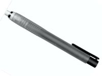
Abrader
Mild abrasive for removing oxides and contaminants.
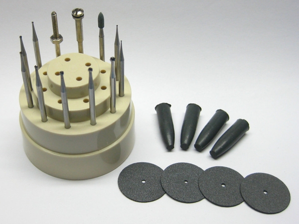
cutting
Ball Mills, Abrasives, Cutting Tools
Ball mills, abrasives and cutting tools for working on circuit boards.
circuit-tracks
Circuit Tracks
Copper conductors to repair circuit board damage including traces and conductors.
235-2106-5
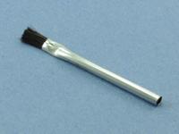
Cleaning Brushes
Disposable brushes for solvent cleaning and application of coatings.
Coatings
Color Agents
Use to tint the color of epoxy used for solder mask repair or circuit base board repair.
115-3302
Circuit Bond Epoxy
Clear, superior strength epoxy in two-compartment plastic packages.
235-3050
High Temp Tape Discs
High temperature polyimide tape discs, .50" diameter.
355-0614
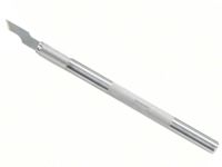
Knife with #16 Blades
A must-have tool for precise cutting, scraping and trimming.
355-3102-5
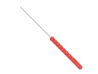
Micro Probes
Sharp probes for dispensing adhesive and positioning small objects.
335-3197
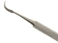
Scraper, Curved Tip
Hardened stainless steel tip for scraping solder mask and removing defects.
Additional Items and Supplies
Cleaner
Cleaner
General purpose cleaner for removing contamination.
Microscope
Microscope
Precision microscope with stand and lighting for work and inspection.
Oven
Oven
General purpose oven for drying, baking and curing epoxies.
Solderinmg Iron
Soldering Iron
Properly maintained soldering iron and properly sized soldering iron tips.
Wipes
Wipes
Nonabrasive, low-linting wipes for cleanup.
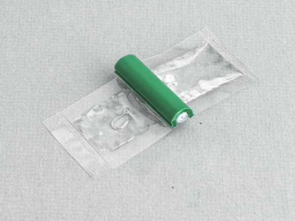
Circuit Bond Epoxy
Circuit Bond is a clear, low viscosity, superior strength epoxy precisely measured out into two-compartment plastic packages, so it's easy to use, and there's no measuring. For over a decade, this high-strength epoxy has been qualified and used by thousands of high-rel electronics manufacturers across the globe.
1. Circuit Bond has a working pot life of 30 minutes. It should not be mixed until ready to use.
2. To use Circuit Bond, remove the plastic clip separating the resin and hardener. Squeeze back and forth from one half of the package to the other to mix the contents.
3. Cut a corner off the package and squeeze all the contents into a Plastic Cup. Stir the contents to ensure it is thoroughly mixed.
4. Circuit Bond may contain bubbles from the mixing process. If needed, use a vacuum system to remove bubbles.
5. Color Agent can be mixed in with Circuit Bond to match surface colors if desired.
6. Apply using a Foam Swab, Micro Probe, or Mixing Stick as required.
7. Cure Circuit Bond for 24 hours at room temperature or 4 hours at 65°C (150°F).
Specifications
Packaging2 gram pre-measured packages
Mix ratio4 parts resin to 1 part hardener
Mix Ratio by Weight (R/H)100/25
ColorClear, transparent
Pot life30 minutes
Cure cycle24 hours at room temp (25 °C) or 4 hours @ 65°C
Thixotropic Index1
Specific Gravity1.20
Percent Solids100%
Viscosity (after mixing)2000 cps
Operating temperature range-55°C to 135°C
Hardness88 Shore D
Lap Shear, Alum to Alum1100 psi
Glass Transition Temperature, Ultimate92°C
Coefficient of Expansion, cm/cm/°C6 E-05
Dielectric strength400 volts/mil
Dielectric Constant, 1KHz@25°C4
Shelf Life6 months minimum
Circuit Tracks
Circuit Tracks are rectangular-shaped conductors made of 99.9% pure CDA 11000 copper. These rectangular ribbons closely conform to the original conductor dimensions. The replacement Circuit Track is bonded in place using epoxy.
Part No. Size
115-5204 115-5204 Circuit Track, .002" x .004" (.051 mm x .102 mm)
115-5205 115-5205 Circuit Track, .002" x .005" (.051 mm x .127 mm)
115-5206 115-5206 Circuit Track, .002" x .006" (.051 mm x .152 mm)
115-5208 115-5208 Circuit Track, .002" x .008" (.051 mm x .203 mm)
115-5210 115-5210 Circuit Track, .002" x .010" (.051 mm x .254 mm)
115-5312 115-5312 Circuit Track, .003" x .012" (.076 mm x .305 mm)
115-5315 115-5315 Circuit Track, .003" x .015" (.076 mm x .381 mm)
115-5520 115-5520 Circuit Track, .005" x .020" (.127 mm x .508 mm)
115-5530 115-5530 Circuit Track, .005" x .030" (.127 mm x .762 mm)
Color Agents
Color Agent is a one-part, air-drying, semi-paste ink commonly used to print hard surfaces, including circuit board base materials. Color Agent can be used to tint the color of epoxy used for solder mask repair or circuit baseboard repair. To use, mix a small amount of color agent with 2 part epoxy as the epoxy is initially mixed. Add more color agents to increase the color intensity if needed.
Part No. Description
115-9102 115-9102 Color Agent, Yellow
115-9185 115-9185 Color Agent, Red
115-9293 115-9293 Color Agent, Blue
115-9348 115-9348 Color Agent, Green
115-9358 115-9358 Color Agent, Light Green
115-9376 115-9376 Color Agent, Medium Green
115-9424 115-9424 Color Agent, Dark Gray
115-9457 115-9457 Color Agent, Light Brown
115-9560 115-9560 Color Agent, Dark Green
115-9561 115-9561 Color Agent, Green
115-9995 115-9995 Color Agent, Black
115-9996 115-9996 Color Agent - White
Images and Figures
4.2.6 Conductor Repair, Inner Layer Method
Damaged Inner Layer
4.2.6 Conductor Repair, Inner Layer Method
Figure 1: Milling into multilayer circuit board to expose the damaged internal circuit.
4.2.6 Conductor Repair, Inner Layer Method
Figure 2: Micro-Drill System used for precision drilling and grinding.

4.2.6 Conductor Repair, Inner Layer Method
Figure 3: cut through the base material, one layer at a time, until the desired inner layer has been reached.
4.2.6 Conductor Repair, Inner Layer Method
Figure 4: Circuit Track in place ready to be soldered.
4.2.6 Conductor Repair, Inner Layer Method
Figure 5: If spacing is critical or the circuit board uses high frequency circuits, bevel the joint as shown.

4.2.6 Conductor Repair, Inner Layer Method
Figure 6: Coat the top and sides of the new circuit with epoxy. Add epoxy until flush with top surface.
4.2.6 Conductor Repair, Inner Layer Method
Figure 7: Completed repair
Procedure
  1. Locate and determine the coordinates where the repair is to be made. Use films or master drawings of the board as needed.
    Note: Obtain as much information as possible on the conductive and non-conductive layers prior to starting the procedure.
  2. Remove components from the immediate area if necessary and clean the area.
  3. Use the microscope and Micro-Drill System and cut through the base material, one layer at a time, until the desired inner layer has been reached. (See Figures 1 and 2)
    Caution: Great care should be taken to prevent further damage to internal circuits.
  4. Each internal circuit should have a flat section exposed to allow the new circuit to be soldered in place. (See Figure 3)
    Note: To reduce damage to the internal circuit, complete the final exposure of the internal circuit using a knife. (See Figure 3)
  5. Remove all loose material. Clean the area.
  6. Apply a small amount of liquid flux to the ends of the internal circuit. Tin the exposed end of each circuit using solder and a soldering iron.
  7. Clean the area.
  8. Select a Circuit Track to match the width and thickness of the circuit to be replaced. Cut a length approximately as needed. The Circuit Track should overlap the existing circuit a minimum of 2 times the circuit width.
  9. Gently abrade the top and bottom of the Circuit Track with the buffer to remove any protective coating and clean.
    Note: If needed, the ends of the Circuit Track may be tinned with solder prior to lap soldering in place.
  10. Place the Circuit Track in position. The Circuit Track should overlap the existing circuit a minimum of 2 times the circuit width. (See Figure 4)
    Note: If the spacing is critical or the circuit Board uses high-frequency circuits, bevel the joint.
    Caution: This bevel joint method may cause problems with circuit Boards exposed to extreme temperature fluctuations.
  11. Apply a small amount of liquid flux to the overlap joint.
  12. Lap solder the Circuit Track to the exposed internal circuit using solder and a soldering iron. Make sure the new circuit is properly aligned.
  13. Clean the area.
    Note: The circuit Board may be preheated prior to filling the area with epoxy. A preheated PC Board will allow the epoxy to easily flow and level out. Epoxy applied to an unheated circuit board may settle below the circuit board surface as the epoxy cures.
  14. Mix epoxy. If desired, add a color agent to the mixed epoxy to match the circuit board color.
  15. Coat the top and sides of the replaced circuit with epoxy. The epoxy bonds the new circuit to the base board material and insulates the circuit. Continue adding epoxy up to the top surface of the circuit board or to the height of the next internal circuit. (See Figure 6)
    Note: A slight overfill of epoxy may be desired to allow for shrinkage when the epoxy cures.
  16. Cure the epoxy per Procedure 2.7 Epoxy Mixing and Handling.
    Caution: Some components may be sensitive to high temperatures.
  17. Add additional Circuit Tracks if needed and coat with additional epoxy.
  18. Continue completing all layers until the top surface of the circuit board is reached. (See Figure 7)
  19. Clean the board as required.
  20. Apply surface coating to match prior coating as required.
Evaluation
  1. Visual examination for alignment and overlap of the new circuit.
  2. Visual examination of epoxy coating for texture and color match.
  3. Electrical tests as applicable.
Procedure for reference only.