This is one of those things that drives people in this business mad. A very expensive and difficult board was successfully manufactured. All the electronic and environmental testing was completed, and the board entered service. Months later, the board began to perform erratically in the field.
Of course, the failure was "high visibility," and everyone was under the gun to find out how and why this was happening. And fix it! After a week or so of testing, the customer urgently directed all possible resources to bear and found the source of this very sneaky problem.
They discovered a dual challenge: a very thick board and leads that were (on occasion) contaminated, most likely oxidized. Only one component type was involved, which was placed at about a dozen locations per board, and not every component demonstrated the problem.
At the affected holes on the through-hole component, barrels were incompletely filled with solder, which caused the solder connection with the component lead to occasionally fail after the board had been in the field working for some time.
When the boards arrived at Circuit Technology Center, our challenge was first to identify the holes that were inadequately filled and then to fill them. At the same time, the customer wanted to ensure that all pins on the problematic part were reflowed to guarantee proper wetting.
Once this was complete, there had to be proof that the holes were filled to everyone's satisfaction. To complicate matters, these boards were covered with a thick conformal coat.
The rather large board was placed, solder side up, at approximately a 30-degree angle to the X-ray emitter head, allowing for a full view of the barrel length. Once the board was in view, each location was photographed, and a marker was placed on the photo noting the holes that were underfilled.
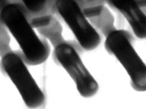
Figure 1 is an example of an X-ray snapshot of a plated hole and leads with insufficient solder.
Now came the hard part. It's easy enough to discuss reflowing ground plan pins on a 0.150-inch-thick, conformal-coated board, but to actually do it? To accomplish this task without damaging non-affected areas, the board had to be prepared by placing thermal-resistant tapes and heat-deflecting material on the surrounding surface areas and components to protect the unaffected components and the solder side conformal coating.
A vacuum desoldering tool removed the conformal coating from the solder-side leads, allowing for flow and fill at those locations. The interesting thing is that this rework was going to be performed on a BGA rework machine to maintain the board at a steady-state high temperature. The machine's bottom heater plates heated the entire substrate, and the topside air nozzle directed heat to the specific rework location.
To maintain control of this volume of heat, thermocouples were placed under the rework locations to monitor the heating of sensitive devices near the rework area.
The board was slowly heated until the proper base temperature was reached. Then, a vacuum desoldering iron was used to suction out the existing solder, removing any suspect material from the barrel.
The final step of the soldering phase was to add solder to the target barrels using the soldering iron and wire solder. This process was repeated until all affected plated through holes were properly filled.
The board was cleaned in a de-ionized water washer. Once again, the board was x-rayed at every location.
The rework environment was hot and demanded great patience and skill from the technicians involved. It ain't always easy, but somebody's got to do it.
Several members of the Circuit Technology Center team contributed to this feature story. Images may be altered or recreated to protect proprietary information.