Gold plating is an ancient technology, and the problems encountered in electronic plating are just as ancient. Things are always changing in this business, getting smaller and more complicated, and sometimes you have to think innovatively to survive. Recently, a customer was in a tough spot due to defective plating. They manufactured a massive backplane measuring over four feet in length and two feet in width. The board is nearly one-half inch thick and plated throughout with gold.
These boards are extremely expensive, and manufacturing them is a nerve-racking experience. Scrapping the boards due to minor problems is demoralizing, not to mention the fact that if you scrap enough of them, you might just be looking for employment somewhere else.
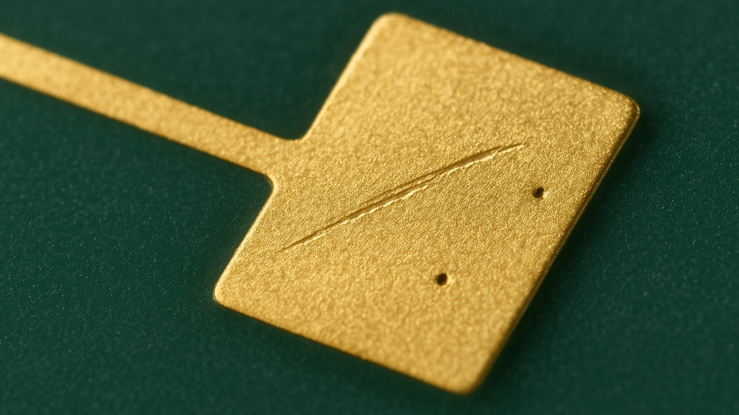
These boards contain thousands of surface-mount pads, and inevitably, one or two have issues. On occasion, the issues are very deep voids or scratches in the pads. (See Figure 1)
We considered two repair options:
- Plate Over
Plate over scratches and voids, leaving the scratch indentation intact while covering the underlying metal with the desired surface finish. Depending on where the void is, how big it is, and your acceptability criteria, this can be all it takes to bring the board to an acceptable condition. On the other hand, this approach may not be accepted if the voids are too big or in a critical area.
To solve the problem, burnish or move the soft surface gold into the void, then touch up the burnished area with selective plating. For slightly larger voids, it may be possible to "blend" the void so that it is difficult to know there was even a defect in the first place.
Conversely, if the scratches are too deep or too wide, it is difficult to bridge the gap without completely deforming the contact surface. Some voids are so large that they cannot be filled using this method. If the above methods don't work, a decision may be made to replace the entire contact.
As you can see by the photo, these are deep voids. Plating over the exposed copper and burnishing these large craters are not acceptable fixes. Unfortunately, this customer could not allow a replacement contact. That left us scratching our heads. - Conductive Paste
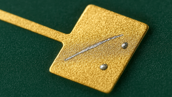
That's when we investigated several conductive pastes that would fill the void, adhere, not shrink, leave no voids due to out-gassing, take the over-plate, and then allow for subsequent soldering. The material we chose met all of the requirements. It was cured at 150 °C, which required some innovative engineering to accomplish on a board as large as a tabletop. (See Figure 2)
We carefully applied the paste using a microscope and a specially honed spatula-style tip. Next, the material was cured. The excess material was carefully removed with another sanding tool, and the surface of the fill material was burnished smooth and even with the surface. This was followed by polishing and, finally, gold plating. (See Figure 3)
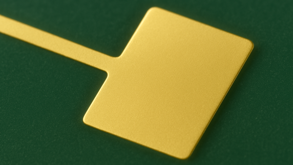
The results were impressive to look at, and the repair went through reflow and testing without incident. We now have a new "Gold Standard" for large void repair.