Manufacturers solder tens of thousands of BGA components every day. Most of this activity occurs during manufacturing and some during rework. Most BGA placement is performed flawlessly. On the other hand, the industry's dynamic forces constantly push the envelope. Occasionally things go wrong.
Circuit board designers are continuously looking for more real estate. That can be as difficult as finding an apartment in Manhattan, but that doesn't stop them from searching.
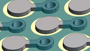
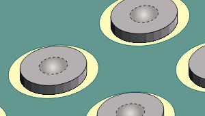
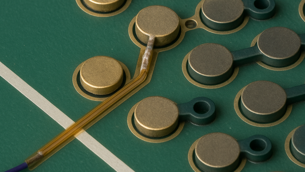
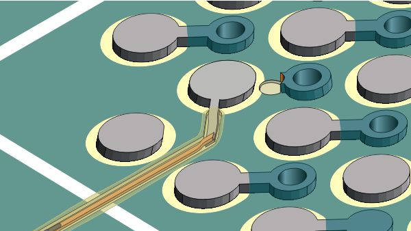
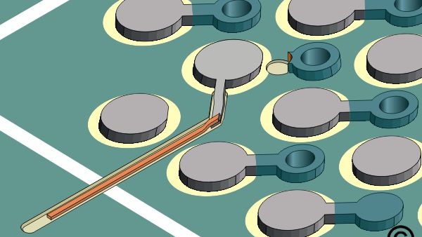
BGA pads used to be routed out to a via on the same side of the board as the pad. Now more and more designers are trying to reclaim that space by using the BGA pad itself as a via. See Figures 1 and 2.
Sometimes the via-in-pad solution disrupts BGA placement. Various technical forums address a number of different issues, but today we'll cover only one: filled vias.
Densely spaced BGA locations present numerous placement challenges. The thermal and electrical characteristics must be carefully calculated and balanced. At a minimum, the site must remain stable when the board is exposed to solder reflow temperatures.
In a recent case, a customer was experimenting with a variety of different fill materials. Variance and voiding in the fill material caused failures in BGA placement. The T sub g variance at one large BGA site caused the board to warp at that location. The warping problem was addressed and solved, but the voiding issue remained.
What's the problem with voiding, you ask? Theoretically, if voids were stable during the thermal transients of BGA rework, there would be no problem, but this is a case where common sense dictates that there will be dynamic forces at work once these voids are exposed to rework temperatures.
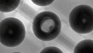
The via is like a long tower with a ball placed on its top. Figure 3 shows what can happen when some of those via voids rise up into the BGA sphere. BGA voiding is a condition that rework personnel battle without accounting for integral via voiding. So adding the via void factor to the rework equation can only aggravate the condition, sometimes with disastrous results.
Figure 3 is a picture of a void that was so volatile that it caused the BGA ball to "blow out". It blew out so forcefully that it deposited a loose piece of solder under the BGA.
Several members of the Circuit Technology Center team contributed to this feature story. Images may be altered or recreated to protect proprietary information.