|
March 11, 2026 |
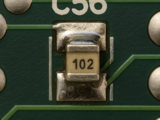
A pad-to-component size mismatch can occur when circuit board artwork errors create pads that do not properly match the intended surface-mount component footprint. In this case, a 1206 chip component was placed on a single elongated pad that was too narrow to meet IPC Class 3 solder joint width requirements. After evaluating alternatives, technicians replaced the incorrect pads with properly sized replacements using a surface-mount pad repair method. Over 60 pads were prepared, bonded, and restored, ensuring the assembly functioned correctly and met reliability requirements.
Feature Story |
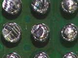
This guide describes the final inspection process for BGA component reballing to verify that solder spheres are properly formed, aligned, and securely attached before the component is reinstalled. Technicians inspect for defects such as crushed or missing spheres, oxidation, substrate damage, contamination, or misalignment. The procedure ensures the reballed component meets IPC and JEDEC requirements and is suitable for reliable use in high-reliability electronic assemblies.
Guide of the Month |
Ball Grid Array (BGA) components often require reballing to restore reliable solder connections or convert lead-free packages to tin-lead alloys required in high-reliability electronics. This technical paper explains the complete process, including deballing, alloy conversion (such as SAC305 to Sn63Pb37), solder sphere replacement, alignment, and reflow. It highlights the use of robotic hot-solder-dip systems, as well as contamination control, inspection, and testing practices needed to ensure defect-free solder joints for aerospace, defense, and other mission-critical applications.
DOWNLOAD |
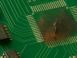
Burn damage to a circuit board's base material can compromise both structural integrity and cosmetic appearance, potentially exposing laminate layers to moisture and contamination. This article explains how technicians remove charred material using precision milling tools, then restore the area with color-matched epoxy. The process rebuilds the laminate surface, protects internal layers, and returns the board to a reliable, professional condition without scrapping the assembly.
Feature Story |
|
Cartoon of the Day
|

|
"I was going to get up early to go running, but my toes voted against me 10 to 1."
Copyright © Randy Glasbergen
|
|
Trivia
The transistor was invented by engineers at Bell Labs. What year was it invented?
See the answer below.
|
Quote of the Week
"If I have seen farther than other men, it is because I stood on the shoulders of giants."
Sir Isaac Newton |
|
|