Outline
This procedure describes the use of flat set eyelets for the repair of a through connection that has an inner layer connect. No surface wire is used. The inner layer reconnect is established by soldering the barrel of an eyelet to the exposed inner layer, and the connection is encapsulated in high-strength epoxy.
Caution: This is a complex repair procedure that demands the proper tools and materials. To expect reliable results, repair technicians must have a high level of expertise. Use this method only when alternative methods are unacceptable.
Caution: This procedure requires very accurate control over the location and depth of a milled hole. It is recommended that a precision drill system be used in combination with a high-power stereo microscope.
Minimum Skill Level - Expert
Recommended for technicians with advanced soldering and component rework skills and extensive experience in most repair/rework procedures.Conformance Level - Medium
This procedure may have some variance with the physical character of the original and most likely varies with some of the functional, environmental and serviceability factors.| Procedure References | |
| 1-0 | 1.0 Foreword |
| 2-1 | 2.1 Handling Electronic Assemblies |
| 2-2 | 2.2 Cleaning Procedures |
Tools and Materials

Ball mills, abrasives and cutting tools for working on circuit boards. |

Clear, superior strength epoxy in two-compartment plastic packages. |

General purpose cleaner for removing contamination. |

Meter and probes to test for electrical continuity. |

Designed for end cutting and hole boring. |

Heavy duty eyelet press designed to set and form eyelets in circuit boards. |

Copper and brass eyelets electroplated with tin designed for repair of plated through holes. |

Sturdy rack for PCBs used for rework and positioning. |

A must-have tool for precise cutting, scraping and trimming. |

Versatile power tool for milling, drilling, grinding, cutting and sanding. |

Precision microscope with stand and lighting for work and inspection. |

Use to provide accurate measurements for thickness and hole diameters. |

Precision drill press for accuracy and controlled depth drilling. |

Used to properly form eyelets used to repair plated holes in circuit boards. |

Used to prepare solder surfaces and to prevent formation of oxides during soldering. |

Properly maintained soldering iron and properly sized soldering iron tips. |

Support base for Setting Tool when forming eyelets for plated hole repair. |

Handy tool has vise jaws to grip small items. |

Nonabrasive, low-linting wipes for cleanup. |
Procedure
Eyelet Selection Criteria
ID - Inside Diameter
The eyelet inside diameter should be a .075 - .500 mm (.003"-.020") greater than the component lead diameter.
OD - Outside Diameter
The clearance hole drilled through the circuit board should allow the eyelet to be inserted without force but should not exceed .125 mm (.005") greater than the eyelet's outside diameter.
LUF - Length Under Flange
The length of the eyelet barrel under the flange should be .630 - .890 mm (.025" - 035"), greater than the thickness of the circuit board. This added length allows for proper protrusion when setting the eyelet.
FD - Flange Diameter
The eyelet flange diameter should be small enough to prevent interference with adjacent lands or circuits.
Note: Be sure to select an eyelet meeting the proper criteria. An eyelet with an oversize flange may interfere with adjacent circuits. An eyelet that is too short will not protrude through the circuit board for proper setting.
Procedure
- Clean the area.
- Select an eyelet using the Eyelet Selection Criteria. Use a pin gauge and caliper to measure the existing plated hole dimensions.
- Pin the circuit board to the base of the Precision Drill System.
- Insert the appropriate ball mill, end mill, or drill into the drill press's chuck.
- Mill or drill out the hole. The drilled hole should be approximately .030 mm (0.001") larger than the eyelet O.D. Inspect to ensure no metallic particles or burrs remain.
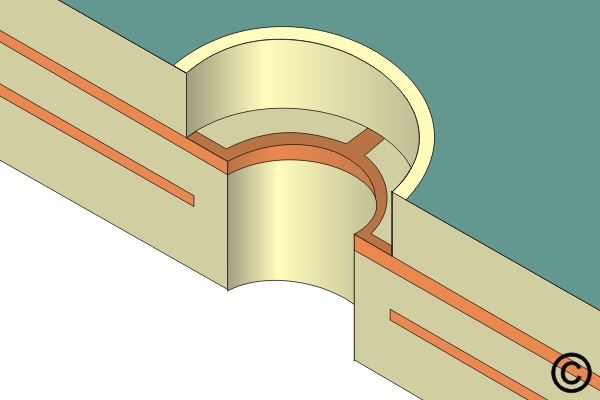
- Select the side of the assembly with a counterbored hole milled into it. This side preferably would have no surface connection.
- Select an end mill approximately .050 - .075 mm (.020" - .030") larger than the eyelet diameter. Insert into the Precision Drill System, mill down to and expose the inner layer signal or plane. (See Figure 1)
Caution: Great care must be taken to control the depth of the milled hole to prevent damage to the inner layer signal or plane. - Clean the area.
- Apply a small amount of flux to the exposed signal or plane and tin with solder.
- Clean the area.
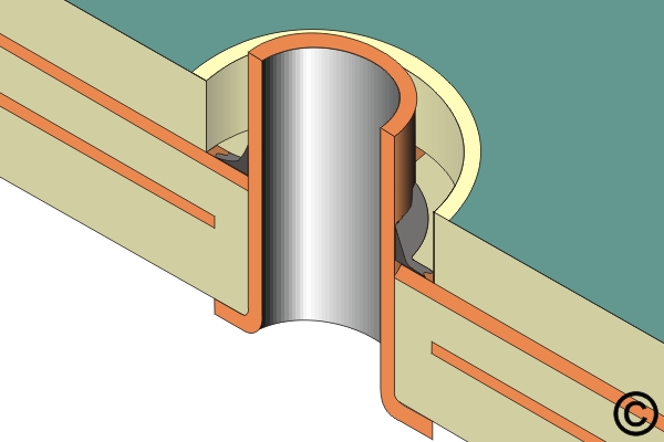
- Insert the eyelet into the hole from the side opposite the milled hole, then apply a small amount of flux into the milled hole.
- Solder the eyelet to the exposed inner layer signal or plane by applying heat from a soldering iron to the barrel of the eyelet. (See Figure 2)
- Completely remove solder flux residue by spraying with cleaner.
- Use a microscope, inspect the solder fillet from the eyelet to the inner connection, and perform electrical tests as required.
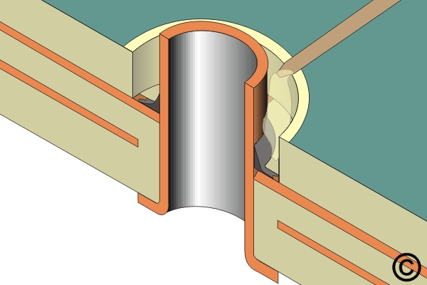
- Mix epoxy as required.
- Fill the milled hole with the epoxy up to and level with the board's surface. (See Figure 3) The epoxy filler material should be free of voids and air bubbles.
- Cure the epoxy per Procedure 2.7 Epoxy Mixing and Handling.
- Select the proper setting tools and insert them into the eyelet press.
- Turn the circuit board over and rest the eyelet flange on the lower setting tool.
- Apply firm, even pressure to flare the eyelet barrel.
- Change the upper setting tool from a flare tool to a flat-end tool. Apply firm, even pressure to flatten the eyelet barrel. (
Note: Inspect the eyelet for evidence of damage. Refer to IPC-A-610 Acceptability of Electronic Assemblies. - Install the component lead and solder, if required.
- Clean the area. (See Figure 9)
Evaluation
- Visual examination of the dimensional requirements of the land diameter and the inside diameter.
- Electrical continuity as required.
Images