Circuit Technology Center and Keysight Technologies have teamed up to provide the test world with a complete turn-key approach for testing DIMMS directly at BGA component sites.
Keysight Technologies W2630A series DDR2 BGA probes enable probing embedded memory DIMMs directly at the ball grid array with the Keysight Technologies logic analyzers and oscilloscopes. Although this dynamic product is available to support Engineers through the test process, it does take some skillful attention.
This procedure provides an overview of the process for installing Keysight Technologies DDR2 DRAM BGA Probes onto circuit board assemblies.
Operator Skills
The DDR2 BGA Probe installation is a challenging process to complete. The engineer or operator must have BGA rework experience. Reballing of the DDR2 BGA Probe is required for placement onto the circuit board. This process also requires experience and skill.
Initial removal of BGA component.
Equipment
BGA reballing kit or system for component and probe solder ball attachment.
Solder paste stencil for circuit board site preparation.
Hot gas rework station designed for BGA component rework.
Microscope with oblique view for perimeter inspection.
X-ray inspection system for post placement inspection.
Step 1: BGA removal from circuit board
The process for safe removal of the BGA component is completed with a Hot Gas Rework Station. The circuit board may require additional preparation, such as baking and masking the area adjacent to the rework site.
To prevent damage, you must closely monitor the temperature of the circuit board with thermocouples during the removal cycle.
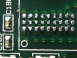
Small corner section of BGA site prior to removal of residual solder.
Step 2: Circuit board site cleaning
After the component has been safely removed from the circuit board, the component and site must be prepared for the probe placement and the BGA onto the probe.
Circuit board and component site cleaning is completed with a vacuum de-soldering nozzle that removes all residual solder from the sites.
Step 3: Solder ball application to Probe and component
The placement of solder balls on the probe and re-balling of the BGA component must be completed before placement on the circuit board. For this process, a specially designed tool for re-balling is used along with specific stencils and solder balls to match the layout of the probe and BGA component.
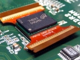
Probe place onto circuit board assembly.
Step 4: Placement of Probe onto circuit board
Installation of the Probe onto the circuit board is completed with Hot Gas Rework System. Solder paste must be applied to the site before placement of the Probe. This process is completed with a solder stencil.
The heat application is controlled by using a repeatable temperature profile that is unique for each circuit board.
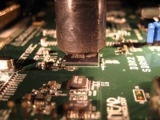
Step 5: Placement of BGA onto the Probe
Installation of the BGA onto the Probe is also completed with Hot Gas Rework System and is very similar to the Probe placement.
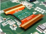
Completed BGA placement onto probe.
The application of heat is controlled by using a repeatable temperature profile. Solder paste must be applied to the site before placement of the Probe. This process is completed with a solder stencil.
Step 6: Inspection to confirm soldering process
Like any BGA application, the process to inspect the solder joints requires an x-ray.
X-ray of the Probe interface to the circuit board and the BGA component to the Probe is required to inspect for solder bridges, voids, and misalignment. Perimeter inspection can be completed with a microscope or inspection camera.
Several members of the Circuit Technology Center team contributed to this feature story.