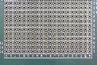
This latest problem is a board fabricated, as shown in Figure 1.
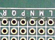
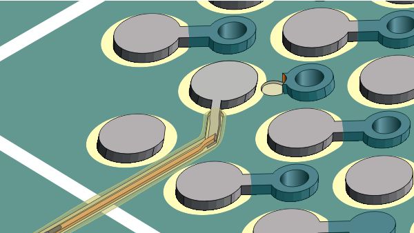
It is unclear in the photo, but plated holes A through V in Row 1 should have been connected to the ground to perform their function properly. They were not connected to each other or ground.
It would seem easy to find a ground point and connect the pins using a wire once the board was populated, but a surface wire was unacceptable.
A connection was needed at the bare board level. This new connection needed to be reliable without impacting the plated-through holes. The full row of plated holes needed to be connected to ground on layer 3.
Here Is The Solution
Using a precision milling system, we milled a groove directly adjacent to the row of pads. Under high magnification, we cleared a small space under the edge of each plated hole pad to provide a connection point. See Figure 2.
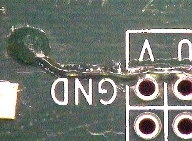
That was nifty work requiring a patient, steady hand. At the end of this row of plated-through holes, we milled down to layer 3 to expose the ground plane for the new bus connection. See Figure 3.
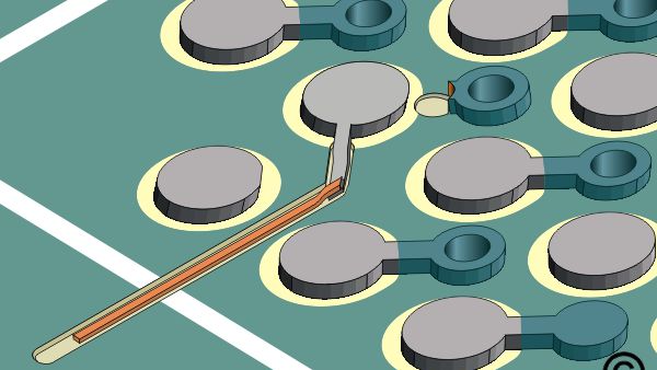
A tinned copper circuit was laid in the machined groove and carefully soldered to the underside of the pad for each plated-through hole. Once that was complete, the circuit was connected to ground.
That rework was visually inspected and electrically tested. Finally, the entire rework area was protected with high-strength thermoset epoxy.
So there it is, good stuff, done right and done quickly. One more fire quenched!
Several members of the Circuit Technology Center team contributed to this feature story. Images may be altered or recreated to protect proprietary information.