Outline
This procedure describes the use of flat set eyelets for the repair of a through connection that has an inner layer connect. No surface wire is used. The inner layer reconnect is established by soldering the barrel of an eyelet to the exposed inner layer, and the connection is encapsulated in high-strength epoxy.
Caution: This is a complex repair procedure that demands the proper tools and materials. To expect reliable results, repair technicians must have a high level of expertise. Use this method only when alternative methods are unacceptable.
Caution: This procedure requires very accurate control over the location and depth of a milled hole. It is recommended that a precision drill system be used in combination with a high-power stereo microscope.
Minimum Skill Level - Expert
Recommended for technicians with advanced soldering and component rework skills and extensive experience in most repair/rework procedures.
Conformance Level - Medium
This procedure may have some variance with the physical character of the original and most likely varies with some of the functional, environmental and serviceability factors.
Cleaner
General purpose cleaner for removing contamination.
Continuity Meter
Meter and probes to test for electrical continuity.
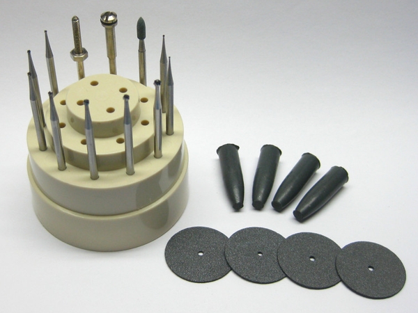
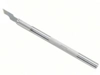
End Mills
Designed for end cutting and hole boring.
Microscope
Precision microscope with stand and lighting for work and inspection.
Pin Gauges
Use to provide accurate measurements for thickness and hole diameters.
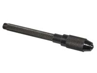
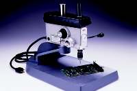
Precision Drill
Precision drill press for accuracy and controlled depth drilling.
Solder Flux
Used to prepare solder surfaces and to prevent formation of oxides during soldering.
Soldering Iron
Properly maintained soldering iron and properly sized soldering iron tips.
Wipes
Nonabrasive, low-linting wipes for cleanup.
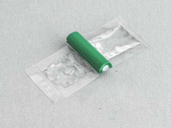
Circuit Bond Epoxy
Circuit Bond is a clear, low viscosity, superior strength epoxy precisely measured out into two-compartment plastic packages, so it's easy to use, and there's no measuring. For over a decade, this high-strength epoxy has been qualified and used by thousands of high-rel electronics manufacturers across the globe.
1.
Circuit Bond has a working pot life of 30 minutes. It should not be mixed until ready to use.
2.
To use Circuit Bond, remove the plastic clip separating the resin and hardener. Squeeze back and forth from one half of the package to the other to mix the contents.
3.
Cut a corner off the package and squeeze all the contents into a Plastic Cup. Stir the contents to ensure it is thoroughly mixed.
4.
Circuit Bond may contain bubbles from the mixing process. If needed, use a vacuum system to remove bubbles.
5.
Color Agent can be mixed in with Circuit Bond to match surface colors if desired.
6.
Apply using a Foam Swab, Micro Probe, or Mixing Stick as required.
7.
Cure Circuit Bond for 24 hours at room temperature or 4 hours at 65°C (150°F).
Specifications
Packaging
2 gram pre-measured packages
Mix ratio
4 parts resin to 1 part hardener
Mix Ratio by Weight (R/H)
100/25
Color
Clear, transparent
Pot life
30 minutes
Cure cycle
24 hours at room temp (25 °C) or 4 hours @ 65°C
Thixotropic Index
1
Specific Gravity
1.20
Percent Solids
100%
Viscosity (after mixing)
2000 cps
Operating temperature range
-55°C to 135°C
Hardness
88 Shore D
Lap Shear, Alum to Alum
1100 psi
Glass Transition Temperature, Ultimate
92°C
Coefficient of Expansion, cm/cm/°C
6 E-05
Dielectric strength
400 volts/mil
Dielectric Constant, 1KHz@25°C
4
Shelf Life
6 months minimum
Eyelets and Tooling
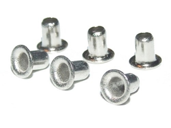
Eyelets are used to repair plated holes in circuit boards and also to create a conductive path through circuit boards for various applications. The eyelets listed below are manufactured from copper or brass and have bright tin plating.
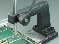
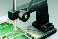
Figure 1: Precision Drill System shown with circuit board pinned in place.
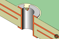
Figure 2: Mill down to and expose inner layer signal or plane.
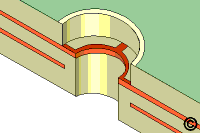
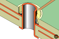
Figure 3: Solder the eyelet barrel to the exposed inner layer signal or plane.
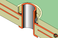
Figure 4: Fill the milled hole with the epoxy up to, and level with, the surface of the board.
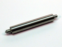
Figure 5: Set the eyelet using an Eyelet Press or using a Tool Grip and Setting Tools.
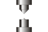
Figure 6: The small cone tip end of the lower Setting Tool faces up. The large cone end of the upper setting tool faces down.
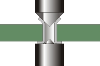
Figure 7: Flare the eyelet barrel using the flare end of the setting tool.
Figure 8: Flatten the eyelet barrel using the flat end of the setting tool.
Figure 9: Eyelet barrel formed flat to circuit board surface.
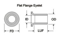
Figure 10: Flat flange eyelet.
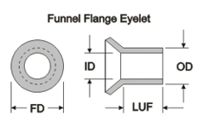
Figure 11: Funnel flange eyelet.
Eyelet Selection Criteria
ID - Inside Diameter
The eyelet inside diameter should be a .075 - .500 mm (.003"-.020") greater than the component lead diameter.
OD - Outside Diameter
The clearance hole drilled through the circuit board should allow the eyelet to be inserted without force but should not exceed .125 mm (.005") greater than the eyelet's outside diameter.
LUF - Length Under Flange
The length of the eyelet barrel under the flange should be .630 - .890 mm (.025" - 035"), greater than the thickness of the circuit board. This added length allows for proper protrusion when setting the eyelet.
FD - Flange Diameter
The eyelet flange diameter should be small enough to prevent interference with adjacent lands or circuits.
Note: Be sure to select an eyelet meeting the proper criteria. An eyelet with an oversize flange may interfere with adjacent circuits. An eyelet that is too short will not protrude through the circuit board for proper setting.
Procedure
Clean the area.
Select an eyelet using the Eyelet Selection Criteria. Use a pin gauge and caliper to measure the existing plated hole dimensions.
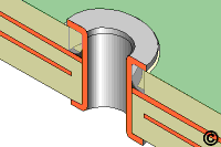
Pin the circuit board to the base of the Precision Drill System. (See Figure 1)
Insert the appropriate ball mill, end mill, or drill into the drill press's chuck.
Mill or drill out the hole. The drilled hole should be approximately .030 mm (0.001") larger than the eyelet O.D. Inspect to ensure no metallic particles or burrs remain.
Select the side of the assembly with a counterbored hole milled into it. This side preferably would have no surface connection.
Select an end mill approximately .050 - .075 mm (.020" - .030") larger than the eyelet diameter. Insert into the Precision Drill System, mill down to and expose the inner layer signal or plane. (See Figure 2)
Caution: Great care must be taken to control the depth of the milled hole to prevent damage to the inner layer signal or plane.
Clean the area.
Apply a small amount of flux to the exposed signal or plane and tin with solder.
Clean the area.
Insert the eyelet into the hole from the side opposite the milled hole, then apply a small amount of flux into the milled hole.
Solder the eyelet to the exposed inner layer signal or plane by applying heat from a soldering iron to the barrel of the eyelet. (See Figure 3)
Completely remove solder flux residue by spraying with cleaner.
Use a microscope, inspect the solder fillet from the eyelet to the inner connection, and perform electrical tests as required.
Mix epoxy as required.
Fill the milled hole with the epoxy up to and level with the board's surface. (See Figure 4) The epoxy filler material should be free of voids and air bubbles.
Cure the epoxy per Procedure 2.7 Epoxy Mixing and Handling.
Select the proper setting tools and insert them into the eyelet press. (See Figure 5)
Turn the circuit board over and rest the eyelet flange on the lower setting tool. (See Figure 7)
Apply firm, even pressure to flare the eyelet barrel. (See Figure 7)
Change the upper setting tool from a flare tool to a flat-end tool. Apply firm, even pressure to flatten the eyelet barrel. (See Figure 8)
Note: Inspect the eyelet for evidence of damage. Refer to IPC-A-610 Acceptability of Electronic Assemblies.
Install the component lead and solder, if required.
Clean the area. (See Figure 9)
Evaluation
Visual examination, the dimensional requirement of land diameter and inside diameter.