The team at Circuit Technology Center was tested when a large OEM discovered a design problem with fifty prototype boards. Two pairs of .005" wide traces had their polarity inverted, needing to be crossed, and time was of the essence.
Reworking these fully populated, 18-layer boards was made even more difficult because these were internal traces, with one pair on layer 4 and the other on layer 18.
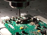
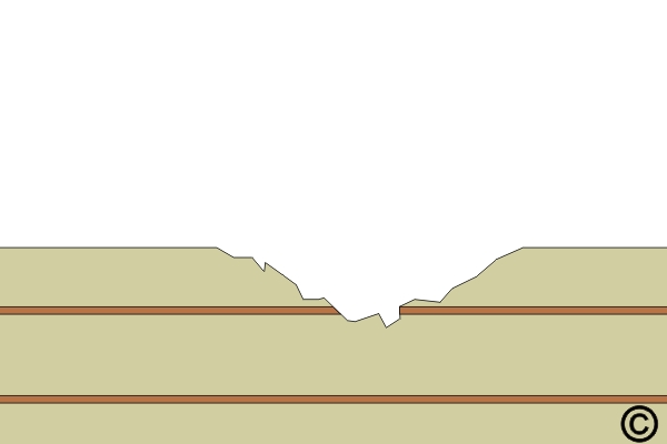
Figure 2: Initially milling.
The boards were placed in a fixture and pinned on a milling machine equipped with a .050" diameter carbide end mill and a stereo microscope. A slot was milled to expose the traces without going so deep that the traces would be damaged. An x-ray system was used to assist in locating the traces. See Figures 1 and 2.
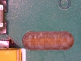
Rework technicians then meticulously scraped away the remaining thin layer of base material using a special knife to expose the copper traces. A small cut was made in each trace, and the remainder of the traces were tinned with solder.
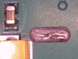
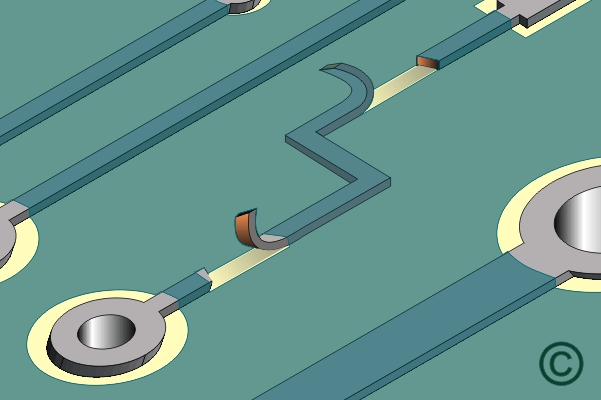
Figure 3: Conductor overlap rework.
A small length of copper ribbon was tinned and then soldered to cross one trace to the other. A piece of approved insulating material was placed above the initial crossover area. Then the second length of tinned copper ribbon was soldered to the other traces to complete the final crossover. See Figure 3.
Finally, the technicians filled each milled area with a high-strength epoxy tinted with a coloring agent.
The process took a knowledgeable team of technicians with steady hands to complete this rework. The final results astounded the customer.
Several members of the Circuit Technology Center team contributed to this feature story.