Everyone loves a good mystery - unless that mystery concerns something important that's missing from your valuable circuit boards! We often discuss methods for repairing circuit boards and components already on the board, but what about replacing surface-mount pads that were never originally intended to be there?
Here's a mystery that could well be called Case of the Missing SMT Pads. In this example, "Whodunit" wasn't as crucial as "Who's gonna fix it in time to meet a shipping deadline?"
A military contractor had a problem. Some SMT pads were missing from some circuit board assemblies. No one could say how or why they had seemingly vanished into thin air, but missiles would not fly unless we could reliably place 2 SMT pads on a batch of boards.
This customer needed two new SMT pads to install a chip capacitor between a surface signal trace and a ground layer. Surface wires were unacceptable.
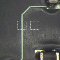
Look at Figure 1, and you'll see where two SMT pads were missing. Adding a pad on the left side was a relatively simple matter, requiring only a surface connection to the conductor.
The pad on the right side, however, was another matter. It needed to be added and connected to the power connection below the surface of the circuit board.
How did we do it?
The first step was to prepare the area. A milling machine outfitted with a .025" end mill was used to accurately remove the thin surface coating at the two individual pad locations and cut out the conductor section where the new pad on the left would be added.
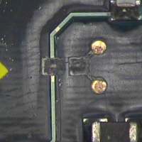
The milling machine was used to spot face down to the ground plane at the two circular locations. (See Figure 2.) This milling procedure is a delicate step and was completed using the precision of a milling machine while the circuit board was properly fixtured.
Next, the short length of the solder mask covering both ends of the severed conductor was scraped away to expose the conductor surface. The two circular spot-faced holes and both ends of the prepared conductor were tinned with solder. This was followed by proper cleaning to remove flux residues.
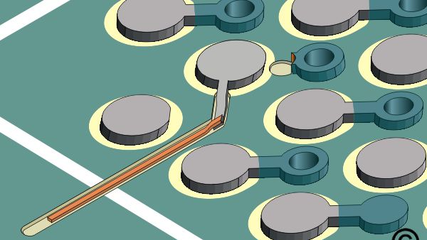
A replacement adhesive-backed surface mount pad was then selected, one with short lengths of conductor protruding from opposite sides of the pad. These conductors naturally lined up with the conductors on the circuit board surface.
A second adhesive-backed replacement surface mount pad was selected, which also had short lengths of conductor that lined up with the spot-faced areas. The adhesive-backed coating was removed from the short sections of the new pads, which would be lap-soldered in a later step.
Let me take a moment to explain these pads. They are not simply pads but a pad replacement system. They are dry-film epoxy-backed replacement copper SMT pads. They are hot-bonded to the circuit board surface, which is better than working with messy liquid epoxies on such small items. This method of SMT pad replacement is covered in the IPC repair and rework guidebook.
The new surface mount pads were placed on the board surface and temporarily held in place with high-temperature tape to accomplish the pad bonding. The tape was removed after a quick application of heat to tack the pad in place. A bonding iron was then used to apply heat and pressure to the new pads, bonding them to the board surface.
The system utilizes special flat tips to cure the adhesive backing in 30 seconds at 500°F. This simple 30-second bonding process fully cured the B-staged adhesive backing on the new pads, ensuring reliable bonding to the circuit board surface.
Once bonding was accomplished, the connecting conductors on the new pads were lap-soldered to the pre-tinned conductors and spot-faced areas on the circuit board. A thorough cleaning followed this soldering procedure.
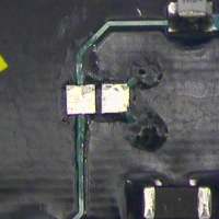
The final step was to over-bond the two small lap joints on the left pad and the two spot-faced areas on the right pad with high-strength thermoset epoxy. (See Figure 3.) This sealed and insulated these connections from further reflow.
Mystery solved... case closed.
Several members of the Circuit Technology Center team contributed to this feature story. Images may be altered or recreated to protect proprietary information.