BGA Conductor Path Re-design
|
|
|
|
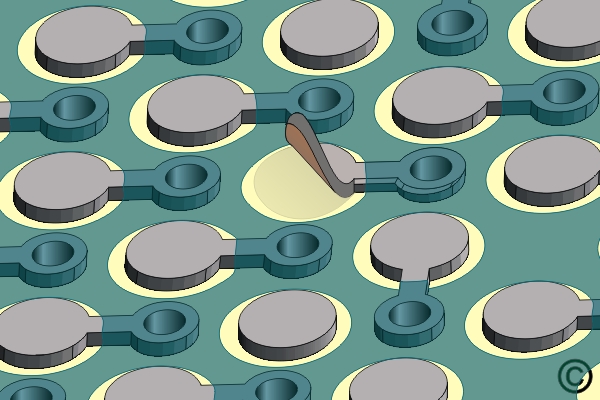
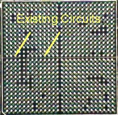
Figure 1: BGA site requiring extensive conductor rtework.
|
This redesign centered around a 676 ball BGA component. A total of 23 of the balls on the BGA were not connected where they needed to be. See Figure 1.
The only viable solution involved re-routing. That's a significant re-design under any circumstances. It would have been easier if the pads that required re-routing were on the perimeter of the BGA layout, but such was not the case.
The newly routed pads had to extend from the center of the component to the outside of the package footprint so that wires could be added to the newly placed pattern of surface mount pads.
All of this is easy enough to consider and doable, but delivering the goods requires attention to detail. First, the design engineers have to determine (electronically) what goes to where then layout engineers have to convert that to usable physical information. See Figure 2.
|
|
|
Figure 2: Proposed routing.
|
That's a good start, but it's only a start. What looks good in a point-to-point drawing may still need some tweaking when it comes to actually lay circuit connections on a board surface.
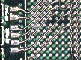
Existing surface conductors and pads caused some re-routing of the circuit paths. As you can see in Figure 3, there are a couple of conductors on the board that is caused concern.
To route the new circuits in the fashion laid out in the supplied drawing would cause the new circuits to be too close to those on the circuit board. Re-routing was called for.
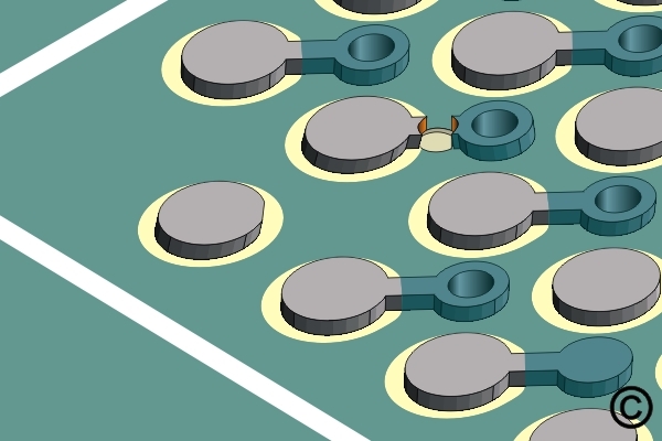
The newly laid circuit must run in such a way as not to interfere with the solder paste stenciling and BGA placement. See Figure 4. The technician used an Xacto knife and a high-speed, precision hand drill to excavate and remove the solder mask to provide a path for the new conductors.
|
|
|
Figure 3: Circuits that interfere with proposed routing.
|
The pad that was originally on the surface of the circuit board was separated from its via, and the original pad was removed from the board. The old BGA pads were and replaced with new pads so that the extending circuit would be oriented in the proper direction.
After the new BGA pads were placed and bonded on the circuit board surface, the new circuit must be run. Following procedure 4.2.1 Conductor Repair, Foil Jumper, Epoxy Method, the circuit is routed out to the perimeter of the BGA footprint.
Routing the copper trace material required patience. Not only did the new conductors need to conform to the many twists and turns of the new path, but they also needed to have the proper height to prevent problems during the replacement of the BGA component.
The last procedure is to place a new surface mount pad on the surface aligned with the extending conductor. Figures 5 and 6 show the final results.
|
|
|
Figure 4: Close-up of completed circuit routing.
|
Close-up, one can see the delicate touch required to properly perform this detailed set of instructions.
Several members of the Circuit Technology Center team contributed to this feature story.
|
|
|
|
|