In circuit board manufacturing, it's not uncommon for specific areas of a board to require additional milling to achieve precise thicknesses. These adjustments are typically handled by the board fabricator before assembly, especially when a board must fit snugly into enclosures, card slots, or under faceplates and bezels.
However, occasional oversights happen. A milling step might be missed or completed inaccurately, resulting in a board that doesn’t meet specifications. When this occurs after assembly has begun—as it did for one major telecommunications company—it creates a more challenging scenario. In that case, the outer edges of the boards were too thick, a deviation that wasn't caught until late in the production process. The boards couldn't be inserted appropriately into their intended slots, and the fix required careful post-assembly milling.
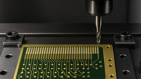
Here's how that edge milling process is performed to bring assembled circuit boards back into spec.
Edge Milling Procedure
- Verify Thickness Specs
Begin by reviewing the fabrication drawing to identify the exact areas that require adjustment and the specified thickness tolerances.
- Secure the Circuit Board Properly
Fixture the board on a flat, stable surface. Use tooling holes for alignment and support the milling area fully—stainless steel bars can help prevent flexing. The board must be tightly clamped to avoid movement. (See Figure 1)
- Set Milling Parameters
Calibrate your depth control, X/Y positioning, and milling speed according to the required cut.
- Choose the Right Tooling
Use an end mill with a diameter equal to or greater than the width of the area you'll be trimming.
- Prepare the Board
Mask off sensitive components or areas that must remain fiber-free during the process.
- Perform the Milling
Mill the edge in a controlled, steady motion, maintaining consistent contact and pressure.
- Verify and Inspect
Use calipers or micrometers to confirm that the newly milled area meets thickness specifications across its entire length.
- Clean Thoroughly
Remove all residual fibers and debris from the circuit board using ESD-safe cleaning methods.
- Final Inspection
Inspect the milled section under at least 5X magnification to ensure precision and cleanliness.
Key Considerations
While edge milling isn't the most complex process, it demands the right environment and equipment: a stable, level surface, a high-precision milling machine, ESD protection, and magnification tools. Most importantly, it requires a skilled operator who understands both the mechanical and electronic sensitivities of circuit board assemblies.
With the right process and experience, circuit boards that are out of spec can still be brought back into proper tolerance spec, saving both the product and the production timeline.
Several members of the Circuit Technology Center team contributed to this feature story. Images may be altered or recreated to protect proprietary information.